

CVD flowable gap fill
a flowable gap and filling technology, applied in the direction of basic electric elements, semiconductor/solid-state device manufacturing, electric apparatus, etc., can solve the problems of void-free filling of high aspect ratio spaces (e.g., ar>3:1) becoming increasingly difficult, and the top part of a high aspect ratio structure sometimes closes
- Summary
- Abstract
- Description
- Claims
- Application Information
AI Technical Summary
Benefits of technology
Problems solved by technology
Method used
Image

Examples
Embodiment Construction
Introduction
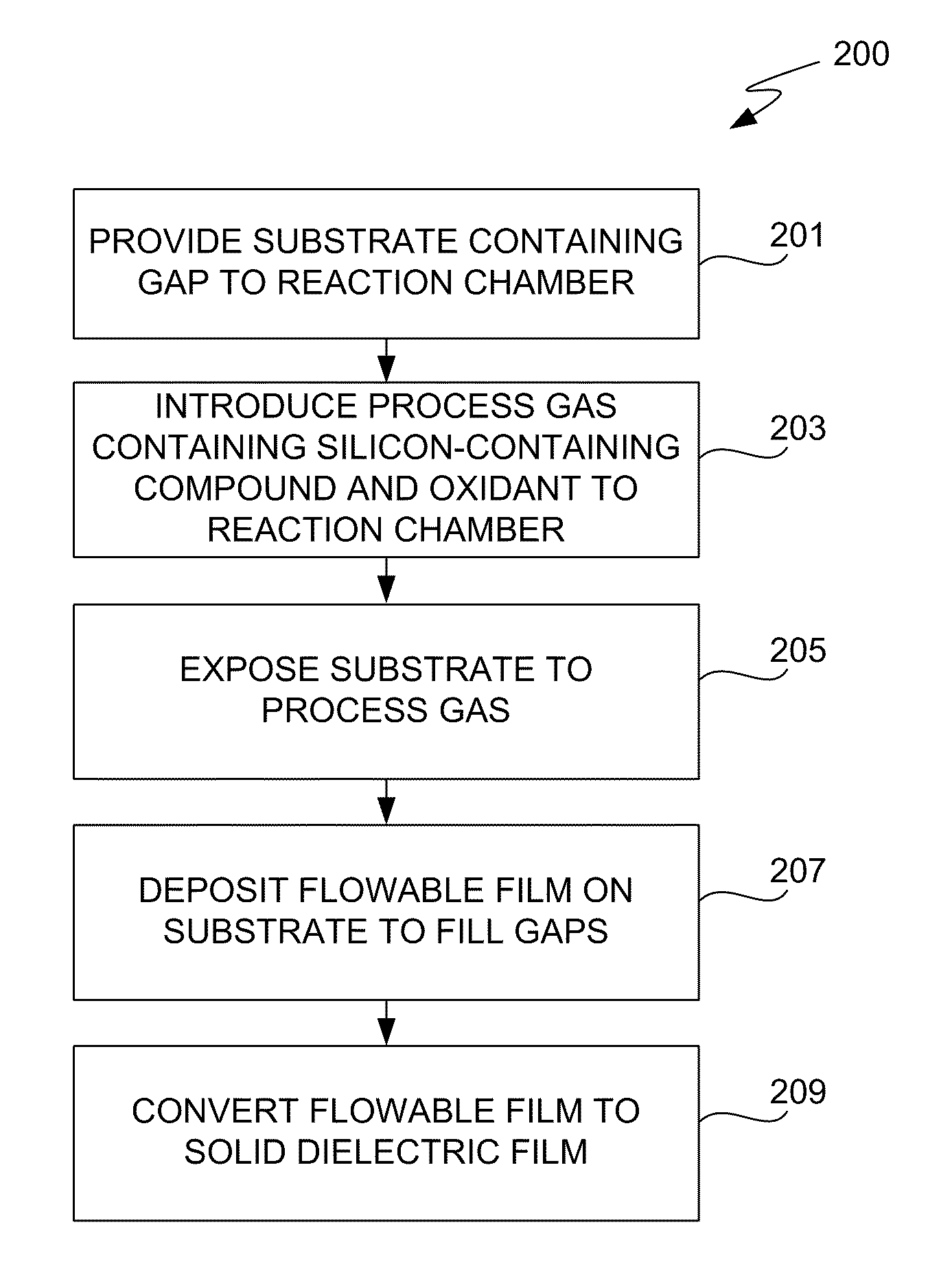
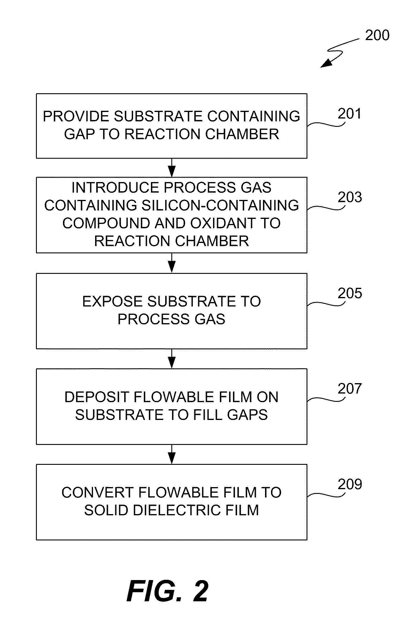
[0020]The present invention relates to deposition processes that provide complete gap of fill high aspect ratio (typically at least 3:1), narrow width gaps.
[0021]Most deposition methods either deposit more material on the upper region than on the lower region of a sidewall or form cusps (also called top-hats) at the entry of the gap. To remove sidewall and top-hat deposits and keep the gap open for further deposition, conventional HDP CVD processes typically use a multi-cycle deposition process—etch process. Each cycle includes a deposition step followed by an etch step Typically, fluorine species are used in the etch step. These fluorine etch steps are costly and time-consuming, in some cases requiring multiple reactors.
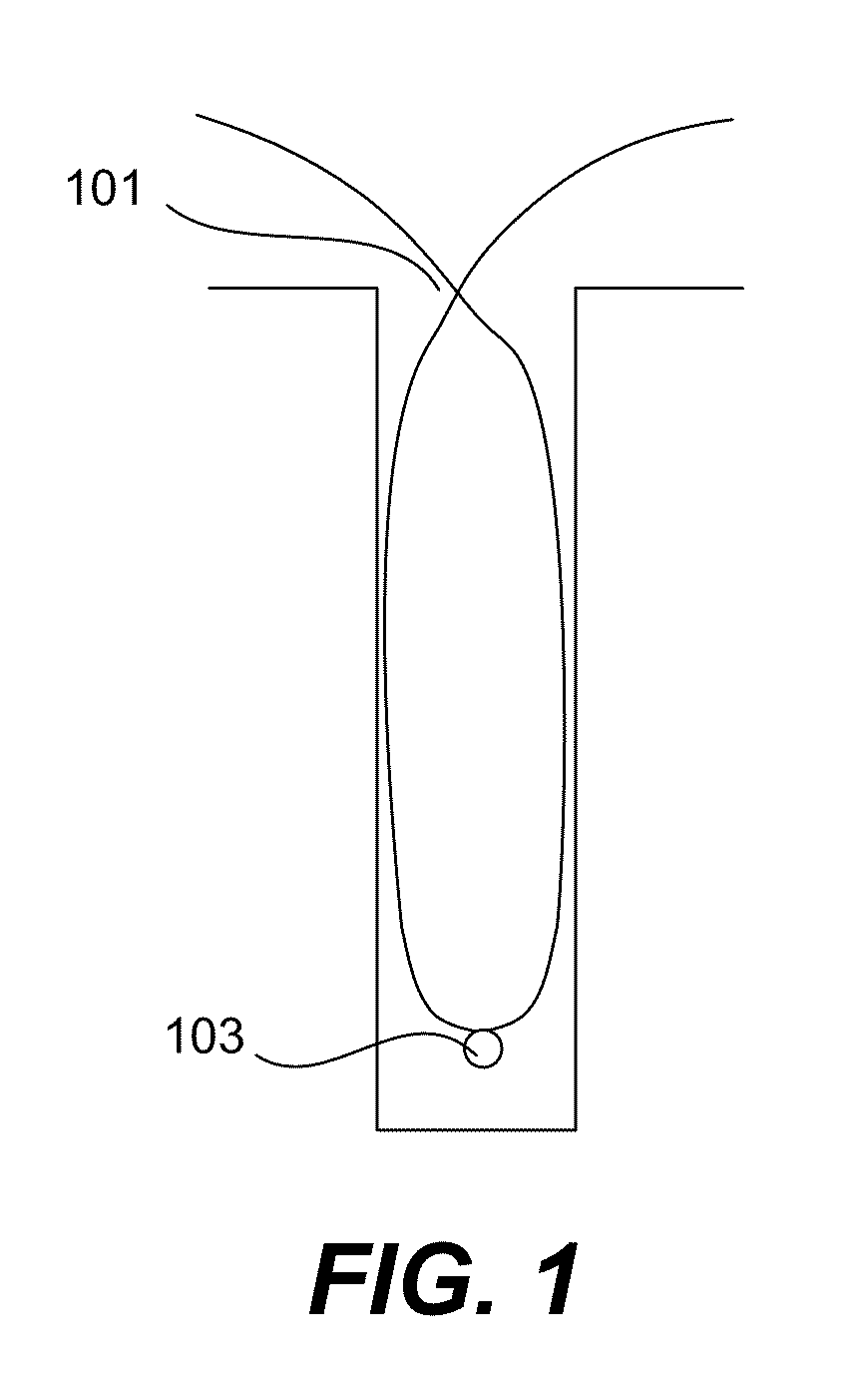
[0022]FIG. 1 shows a rough schematic of a trench partially filled by a conventional HDP CVD method. Reference number 101 indicates where sidewalls have formed from film that has been sputtered away from the bottom of the trench and redeposited on the sid...
PUM
 Abstract
Description
Claims
Application Information