Composite high reflectivity layer

a high reflectivity, contact technology, applied in the direction of mirrors, semiconductor devices, electrical devices, etc., can solve the problems of light being absorbed by the reflector cup, optical loss may occur when the light is reflected, and limited external quantum efficiency, so as to achieve a higher reflectivity layer and increase emission efficiency

Active Publication Date: 2011-03-29
CREELED INC
View PDF23 Cites 41 Cited by
  • Summary
  • Abstract
  • Description
  • Claims
  • Application Information

AI Technical Summary

Benefits of technology

[0012]The present invention discloses a higher reflectivity layer for use in LEDs and LED chips to increase emission efficiency. One embodiment of a light emitting diode (LED) chip according to the present invention comprises an active region between two oppositely doped layers. A composite high reflectivity layer is arranged to reflect light emitted from the active region. The composite layer comprises a first layer, one or more second layers, and a plurality of third layers on the first layer. The second layers have an index of refraction different from the third layers. The second and third layers alternate, and each of the third layers having different thicknesses compared to the other of the third layers. A reflective layer is included on the topmost of the second and third layers

Problems solved by technology

For conventional LEDs with a single out-coupling surface, the external quantum efficiency can be limited by total internal reflection (TIR) of light from the LED's emission region.
While the reflective cup 13 may direct light in an upward direction, optical losses may occur when the light is reflected.
Some light may be absorbed by the reflector cup due to the less than 100% reflectivity of practical reflector surfaces.
The reflectivity at 0 degrees is lower than the reflectivity at 90 degrees, and this difference can result in up to 5% or more of the light being lost on each reflection.
In a LED chip, in some instances TIR light can reflect off the mirror several times before it escapes and, as a result, small changes in the mirror absorption can lead to significant changes in the brightness of the LED.

Method used


Image

  • Composite high reflectivity layer
  • Composite high reflectivity layer
  • Composite high reflectivity layer

Examples


Embodiment Construction

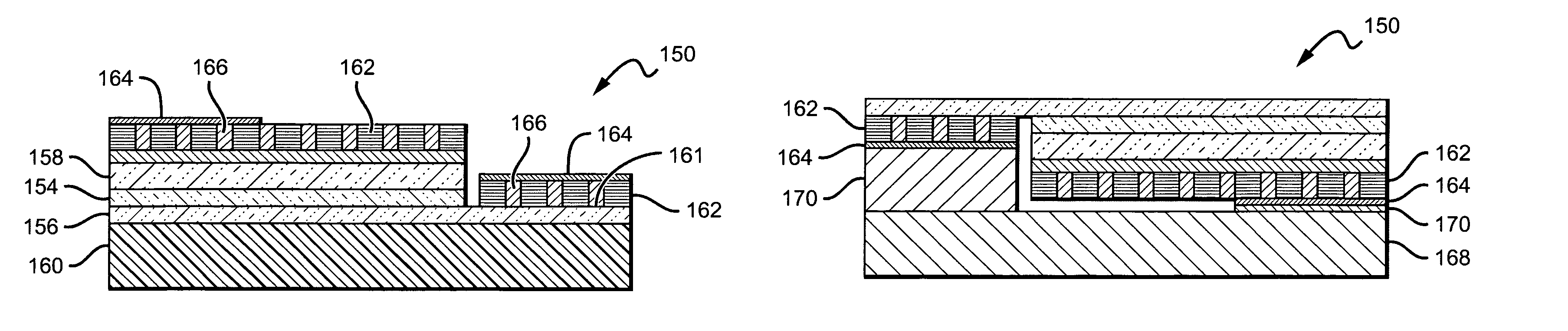
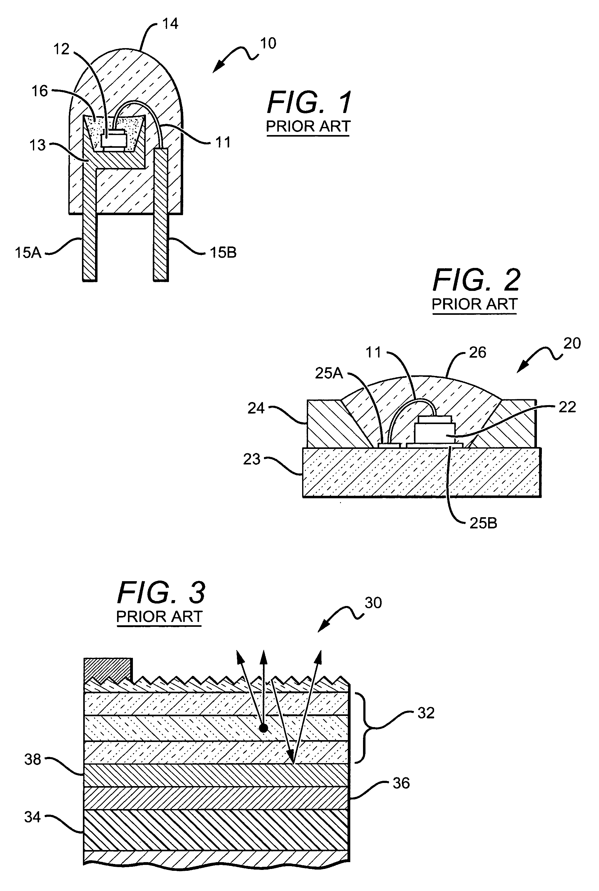
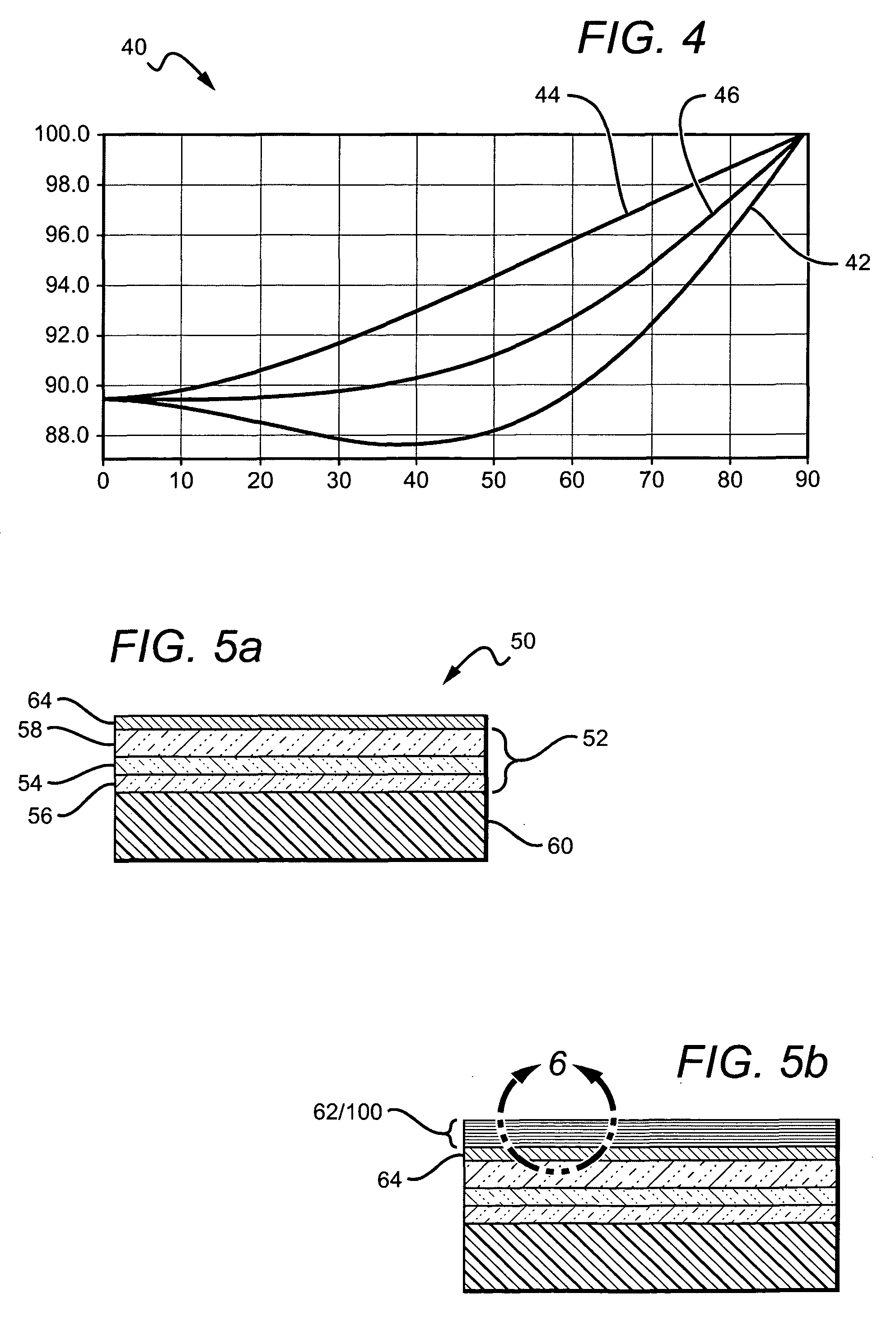
[0037]The present invention is directed to solid-state emitters and methods for fabricating solid-state emitters having one or more composite high reflectivity contacts or layers arranged to increase emission efficiency of the emitters. The present invention is described herein with reference to light emitting diodes (LED or LEDs) but it is understood that it is equally applicable to other solid-state emitters. The present invention can be used as a reflector in conjunction with one or more contacts, or can be used as a reflector separate from the contacts.

[0038]The improved reflectivity of the composite contact / layer (“composite layer”) reduces optical losses that can occur in reflecting light that is emitted from the active region in a direction away from useful light emission, such as toward the substrate or submount, and also to reduce losses that can occur when TIR light is reflecting within the LED. Embodiments of the present invention provide various unique combinations of la...


PUM


Abstract

A high efficiency light emitting diode with a composite high reflectivity layer integral to said LED to improve emission efficiency. One embodiment of a light emitting diode (LED) chip comprises an LED and a composite high reflectivity layer integral to the LED to reflect light emitted from the active region. The composite layer comprises a first layer, and alternating plurality of second and third layers on the first layer, and a reflective layer on the topmost of said plurality of second and third layers. The second and third layers have a different index of refraction, and the first layer is at least three times thicker than the thickest of the second and third layers. For composite layers internal to the LED chip, conductive vias can be included through the composite layer to allow an electrical signal to pass through the composite layer to the LED.

Description

BACKGROUND OF THE INVENTION[0001]1. Field of the Invention[0002]This invention relates to light emitting diodes, and to light emitting diodes with a high reflectivity contact and method for forming the contact.[0003]2. Description of the Related Art[0004]Light emitting diodes (LED or LEDs) are solid state devices that convert electric energy to light, and generally comprise one or more active layers of semiconductor material sandwiched between oppositely doped n-type and p-type layers. When a bias is applied across the doped layers, holes and electrons are injected into the active layer where they recombine to generate light. Light is emitted from the active layer and from all surfaces of the LED.[0005]For typical LEDs it is desirable to operate at the highest light emission efficiency, and one way that emission efficiency can be measured is by the emission intensity in relation to the input power, or lumens per watt. One way to maximize emission efficiency is by maximizing extracti...

Claims


Application Information

Patent Timeline
Patent Type & Authority Patents(United States)
IPC IPC(8): H01L33/00
CPCH01L33/10H01L33/46H01L2224/48091H01L2224/48247H01L2924/00014G02B5/08
Inventor LI, TINGHANSEN, MONICAIBBETSON, JAMES
Owner CREELED INC
Why Eureka
Try Eureka