
Transferable antireflection material for use on optical display
a technology of anti-reflection materials and optical displays, applied in the field of anti-reflection materials, can solve the problems of reducing the surface energy of the coating layer, reducing the interfacial adhesion of the fluoropolymer layer to the other polymer or substrate layer, and reducing the viscosity of polymeric materials, so as to achieve good durability, reduce the effect of refractivity and good adhesion
- Summary
- Abstract
- Description
- Claims
- Application Information
AI Technical Summary
Benefits of technology
Problems solved by technology
Method used
Image

Examples
example 1
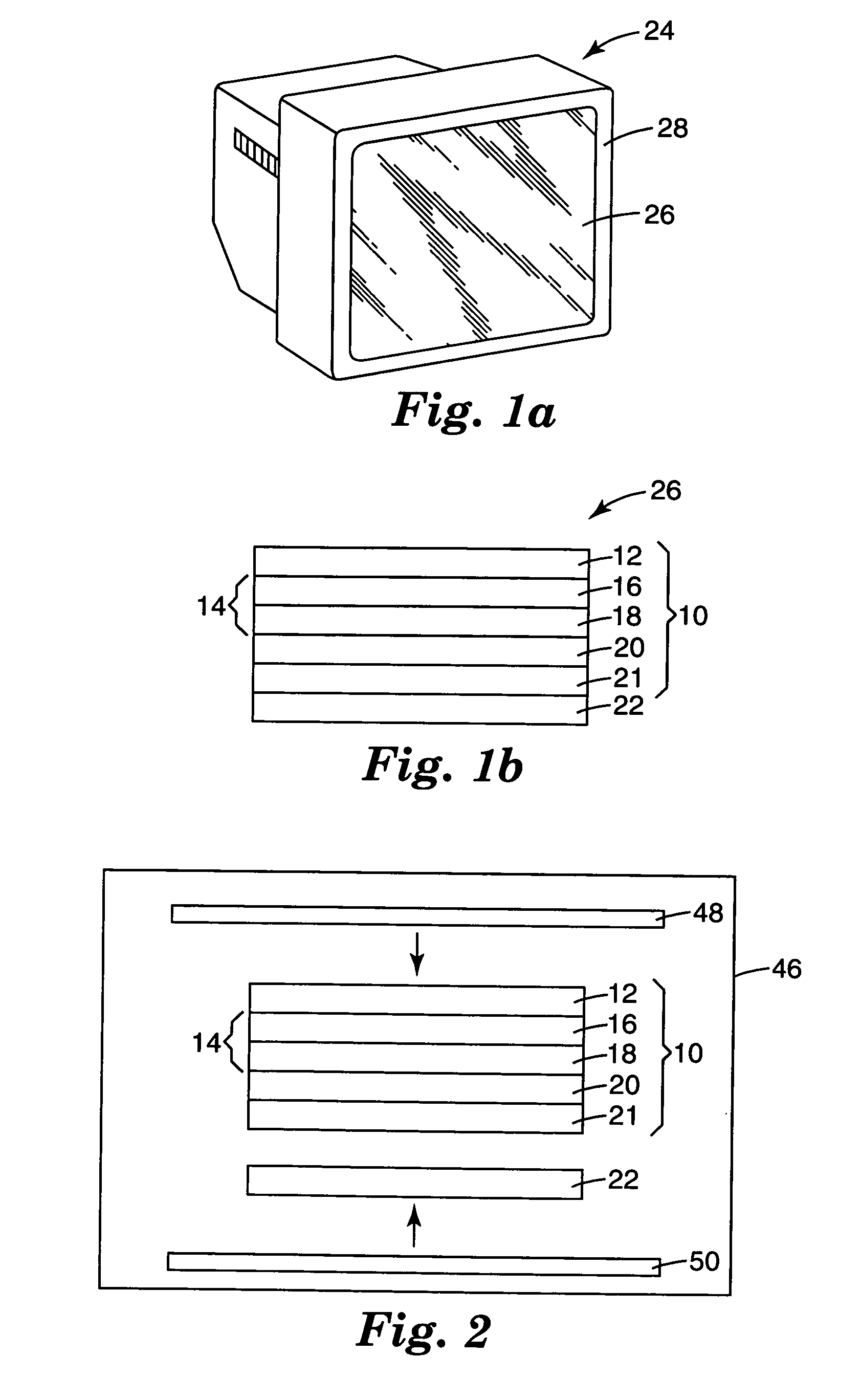
[0091] On 75 um PET (Product name: O-75, Teijin), L-1 described above was coated by Mayer bar #6 and dried in 80° C. oven for 30 seconds and then put in 120° C. oven for 20 seconds to make a low index layer with approximately 90 nm thickness. On the low index layer, H-1 was coated by Mayer bar #8 and dried in 80° C. oven for 30 seconds and then put in 120° C. oven for 20 seconds. The H-1 coated film was UV exposed for 8 seconds from the PET release layer side with a 120 W Fusion lump (D bulb) under nitrogen gas atmosphere to make a high index layer with approximately 130 nm thickness. On the high index layer, HC-1 was coated by Mayer bar #10 and dried in 80° C. oven for 60 seconds. This coated film was UV exposed for 8 seconds from the PET release layer side with a 120 W Fusion lump (D bulb) under N2 atmosphere to make hard coating layer with approximately 5 um thickness. Moreover, on the hard coating layer, Adh-1 was coated by Mayer bar #9 and dried in 80° C. oven for 60 seconds to...
example 2
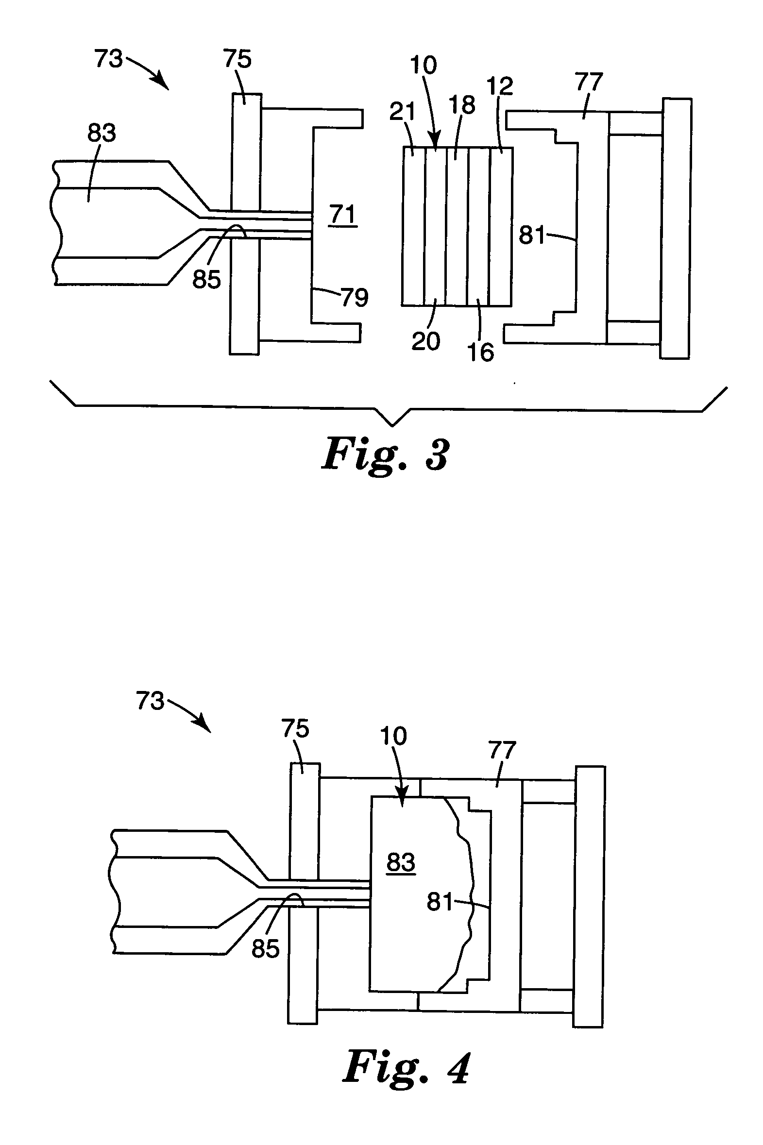
[0093] TAR-1 in Example 1 was inserted into a molding die and PMMA was injection molded with 240° C. injection temperature. The pressed materials were taken out and PET film was removed after cooling. As a result, the anti-reflection layer was successfully transferred on the molding surface.
example 3
[0094] The same procedure was taken to make TAR-2 except using H-3 in Example 1.
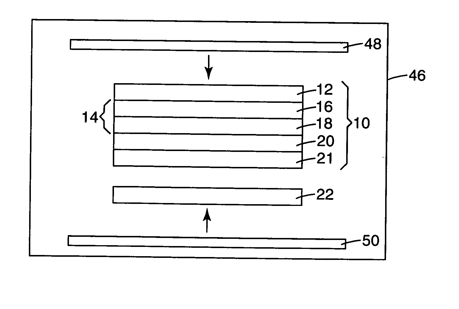
[0095] In the next step, TAR-2 and a commercial acrylic board with 7 cm square and 2 mm thickness were put together and inserted into a heat-press machine with two metal plates and heat-pressed for 40 seconds with 30 MPa pressure. The temperatures of the plates were 180° C. for film / acrylic side and 50° C. for the opposite side. The pressed materials were taken out and PET film was removed after cooling. As a result, the anti-reflection layer was successfully transferred on the acrylic surface.
PUM
| Property | Measurement | Unit |
|---|---|---|
| wavelength | aaaaa | aaaaa |
| refractive indices | aaaaa | aaaaa |
| refractive index | aaaaa | aaaaa |
Abstract
Description
Claims
Application Information