
Epitaxial thin films

a thin film, epitaxial technology, applied in the direction of thin/thick film capacitors, final product manufacturing, fixed capacitors, etc., can solve the problems of ybco, prior methods and products cannot compare to the cost reduction, and wire also suffers from performance limitations, etc., to achieve high permittivity, low loss for use, and high permittivity

Inactive Publication Date: 2006-04-25
MICROCOATING TECH +2
View PDF10 Cites 18 Cited by
  • Summary
  • Abstract
  • Description
  • Claims
  • Application Information

AI Technical Summary

Benefits of technology

CCVD processes provide high-quality, epitaxial films with improved performance and reduced manufacturing costs, enhancing the potential for widespread use in high-temperature superconductors, solid oxide fuel cells, and gas separation membranes, while also enabling the production of high-permittivity dielectric layers for capacitors.

Problems solved by technology

Even the most promising forecasts for mass production cost of state-of-the-art HTSC powder-in-tube wire are well in excess of this target; this wire also suffers from performance limitations.
Prior methods and products cannot compare to the reduced expense and the flexibility of the CCVD methods and high quality epitaxial buffer layers produced thereby.
However, “weak link” or dissipative behavior at grain boundaries within the current path for YBCO has been this material's major limitation.
However, all of these methods have expense and scalability limitations.

Method used


Image

  • Epitaxial thin films
  • Epitaxial thin films
  • Epitaxial thin films

Examples


example 1

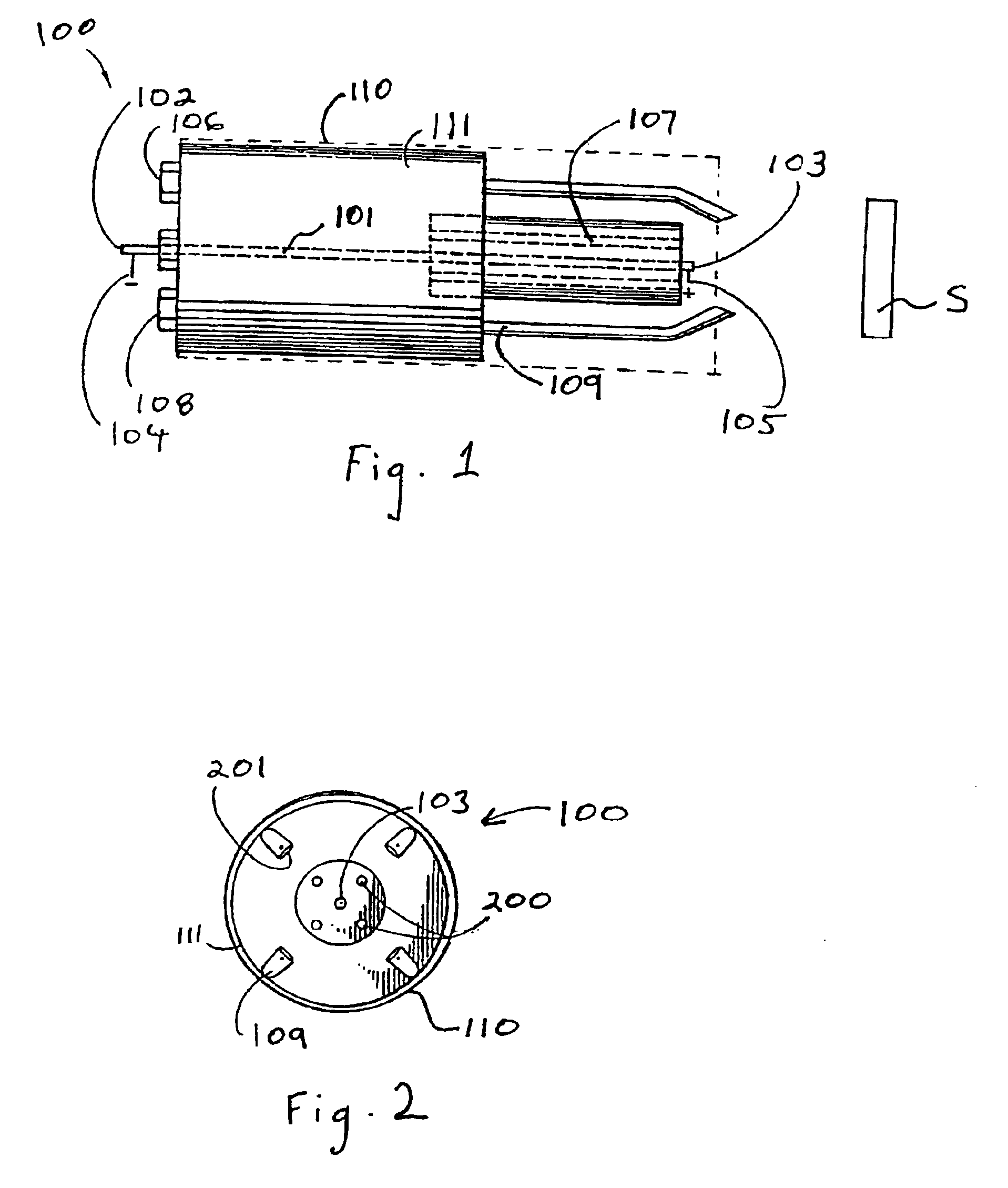
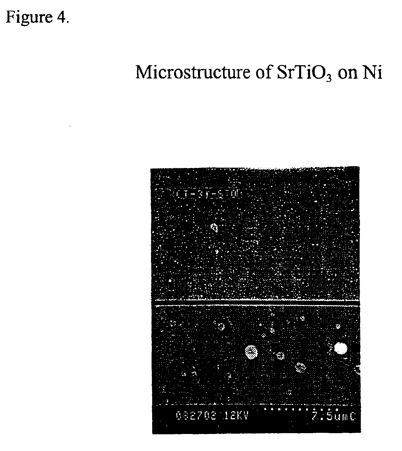
[0046]In this example, SrTiO3 (STO) was deposited on roll textured Ni. The precursor solution included 1.26 g of Sr-2-ethylhexanoate (2eh) (diluted with toluene to 1.5 wt % Sr), 1.11 g of Ti-di-I-propoxide bis acetylacetonate (diluted with isopropanol to 0.94 wt % Ti), 51 ml denatured ethanol and 300 g of propane. This solution was fed to the needle at a rate of 3 ml / min., while supplying 1.75 amps of heating current to the needle. Tip oxygen at 80 psi was supplied at a rate of 3 lpm, pilot hydrogen at 15 psi was supplied at a rate of 18 lpm and argon at 50 psi was used as the shield gas at a rate of 32 lpm. The deposition was conducted for 10 minutes with a substrate temperature of 950° C.

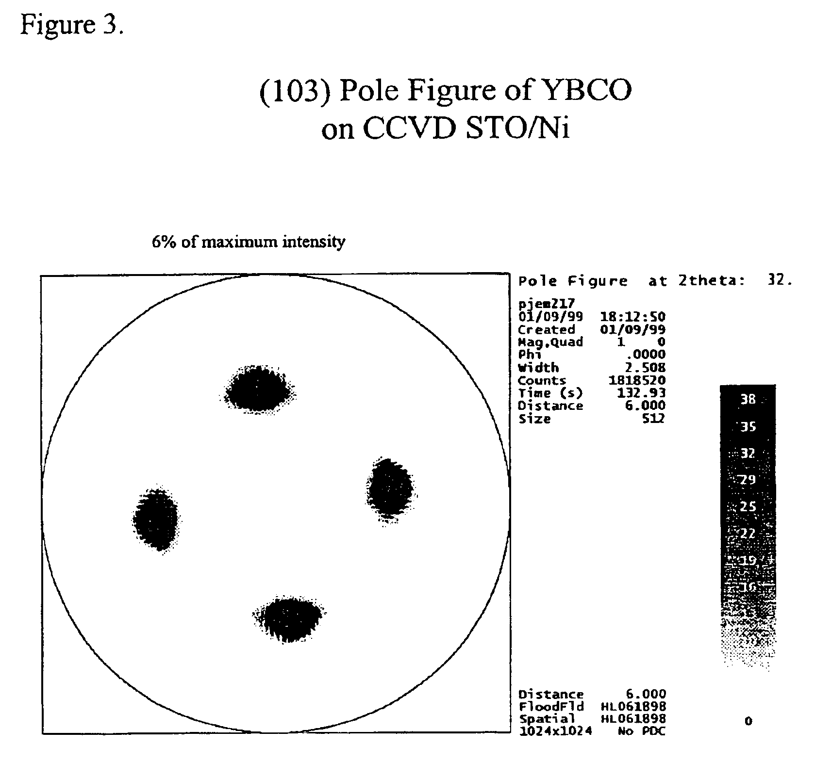
[0047]The deposited buffer layer was highly epitaxial and exhibited a single cube in-plane orientation as shown in FIG. 3. FIG. 3 is a pole figure of a YBa2Cu3Ox (YBCO) superconductor deposited on top of the CCVD deposited SrTiO3 buffer layer on Ni. The pole figure of the YBCO layer is exhibiting ...

example 2

[0056]In this example, LSM was deposited on a-plane sapphire using CCVD. The precursor solution comprised 0.21 g Mn-2eh (diluted with mineral spirits to wt % 6 wt % Mn), 1.96 g La-2eh (diluted with mineral spirits to 2 wt % La), 0.97 g Sr-2eh (10 wt % Sr in 2-ethylhexanoic acid and further diluted with toluene to 1.25 wt % Sr). This solution was added to toluene for a total volume of 10 ml, and then added to 60 g propane. This solution was fed at a rate of 3 ml / mn. for a total deposition time of 30 min. 2.42 amps of current were supplied to the needle with 3500 ml / min. of tip oxygen. Tip oxygen was 60 psi (with no hydrogen or argon). The flame temperature was maintained at 1200-1400 degrees C. In FIG. 8, the SEM micrograph of LSM on sapphire shows a porous and columnar microstructure. The porosity of the electrode layer must be sufficient for the transport of gaseous species or ions to the electrolyte while allowing for the collection of electrons from the associated electrochemical...

example 3

[0057]In this example, YSB was deposited on a-plane sapphire using CCVD. The precursor solution comprised 2.88 g Ba-2eh (8.5 wt % Ba in xylene and further diluted with toluene to 2 wt % Ba), 0.08 g Y-2eh (diluted with toluene to 0.69 wt % Y). This solution was added to toluene for a total volume of 10 ml, and then added to 60 g propane. This solution was fed at a rate of 3 ml / min. for a total deposition time of 29 min. 2.50 amps of current were supplied to the needle with 3300 ml / min. of tip oxygen. The flame temperature was maintained at 1200 degrees C. Tip oxygen was 60 psi (with no hydrogen or argon).


PUM

PropertyMeasurementUnit
thicknessaaaaaaaaaa
temperaturesaaaaaaaaaa
pressuresaaaaaaaaaa

Abstract

Epitatial thin films for use as buffer layers for high temperature superconductors, electrolytes in solid oxide fuel cells (SOFC), gas separation membranes or dielectric material in electronic devices, are disclosed. By using CCVD, CACVD or any other suitable deposition process, epitaxial films having pore-free, ideal grain boundaries, and dense structure can be formed. Several different types of materials are disclosed for use as buffer layers in high temperature superconductors. In addition, the use of epitaxial thin films for electrolytes and electrode formation in SOFCs results in densification for pore-free and ideal gain boundary / interface microstructure. Gas separation membranes for the production of oxygen and hydrogen are also disclosed. These semipermeable membranes are formed by high-quality, dense, gas-tight, pinhole free sub-micro scale layers of mixed-conducting oxides on porous ceramic substrates. Epitaxial thin films as dielectric material in capacitors are also taught herein. Capacitors are utilized according to their capacitance values which are dependent on their physical structure and dielectric permittivity. The epitaxial thin films of the current invention form low-loss dielectric layers with extremely high permittivity. This high permittivity allows for the formation of capacitors that can have their capacitance adjusted by applying a DC bias between their electrodes.

Description

RELATED CASES[0001]This application claims priority to U.S. Provisional Patent Application Ser. No. 60 / 115,519, filed Jan. 12, 1999, which is hereby incorporated by reference, in its entirety.GOVERNMENT CONTRACT[0002]The United States Government has rights in this invention pursuant to Contract No. F33615-98-C-5418 awarded by the United States Department of Defense, and Contract Nos. DE-FG02-97ER82345, ACQ-9-29612-01 and 4500011833 awarded by the United States Department of Energy.FIELD OF THE INVENTION[0003]The invention relates to epitaxial thin films, and more particularly to epitaxial thin films for use as, inter alia, buffer layers for high temperature superconductors, electrolytes in solid oxide fuel cells (SOFC), gas separation membranes or dielectric material in electronic devices.BACKGROUND OF THE INVENTION[0004]While the ability to deposit epitaxial coatings on textured substrates has been demonstrated in the past, the methods to produce these coatings have several disadva...

Claims


Application Information

Patent Timeline
Patent Type & Authority Patents(United States)
IPC IPC(8): B05D5/12B32B9/00B32B15/04
CPCB01D53/228B01D71/024C23C16/453H01G4/1209H01G4/33H01M8/124B01D67/0072Y10T29/5313B01D2256/12H01M8/0687H01M8/1253Y02E60/521Y02E60/525B01D2325/22B01D2325/26Y10T29/53135Y10T29/53204Y10T29/532Y10T29/49115Y02E60/50Y02P70/50B01D71/0271
Inventor HUNT, ANDREW TYEDESHPANDE, GIRISHLIN, WEN-YIJAN, TZYY-JIUAN
Owner MICROCOATING TECH
Learn More