Eureka AIR delivers breakthrough ideas for toughest innovation challenges, trusted by R&D personnel around the world.

Semiconductor manufacturing device

a manufacturing device and semiconductor technology, applied in the field of semiconductor manufacturing devices, can solve the problems of increasing environmental burden, affecting the manufacturing cost, and inevitably large size of mother glass, so as to improve the usability of materials, reduce the space of manufacturing lines, and reduce the effect of productivity and manufacturing cost reduction

Inactive Publication Date: 2011-04-12
SEMICON ENERGY LAB CO LTD
View PDF78 Cites 0 Cited by
  • Summary
  • Abstract
  • Description
  • Claims
  • Application Information

AI Technical Summary

Benefits of technology

[0023]The invention having the abovementioned configuration enables to improve reduction in a space of a manufacturing line and efficiency, contributes to significant quality improvement, productivity improvement and manufacturing cost reduction in manufacturing a display panel, and provides a method for forming a wiring pattern or a contact hole adapted to the earth environment and a method of manufacturing various deposition devices and display devices. In addition, high-speed and continuous treatment is possible because the invention is an atmospheric pressure method which can perform in-line treatment coupled with production. Moreover, there are few unnecessary materials because only a required amount of materials may be used in a desired part. Therefore, usability improvement of a material as well as reduction in manufacturing expense can be achieved.

Problems solved by technology

In other words, most of the material are thrown, which not only affects the manufacturing cost, but also increased environmental burden.
This is because glass which flows to a manufacturing line, so-called mother glass becomes inevitably large in size.
In addition, as the size of a substrate gets larger, a manufacturing apparatus also becomes inevitably larger.
Therefore, an extremely large floor space is needed.
In particular, aside from jumboizing of a film formation chamber, scale of a supplementary vacuum pump or the like also gets larger because a film formation process is essentially performed in vacuum; therefore, an occupied area of the device gets large limitlessly.

Method used


Image

  • Semiconductor manufacturing device
  • Semiconductor manufacturing device
  • Semiconductor manufacturing device

Examples


embodiment mode 1

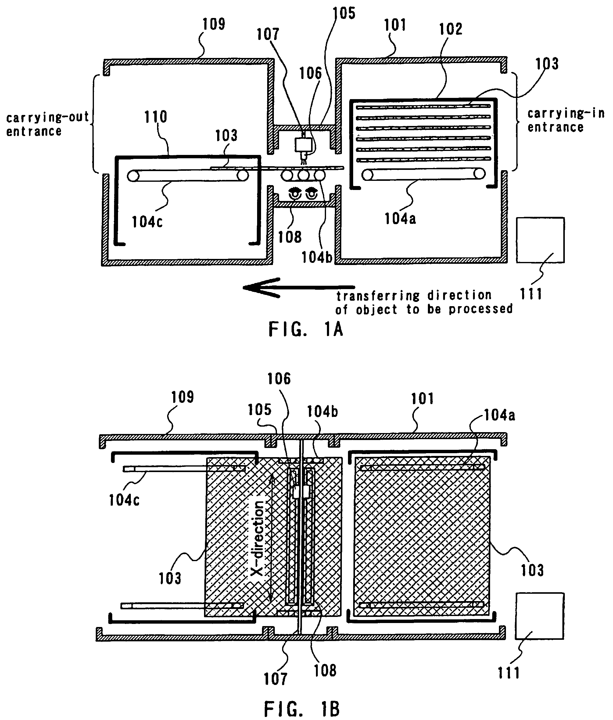
[0040]First, as a feature of the present invention, performing deposition treatment or etching treatment under atmospheric pressure or adjacent to atmospheric pressure (5 to 800 Torr, 6.6×10² to 1.1×10⁵ Pa) by using a plasma generating means is given. As an example of plasma treatment apparatus used in the invention, apparatus having a cylindrical electrode having a nozzle-shaped narrow opening at a tip thereof, in which a first electrode surrounds a second electrode, is described with reference to FIG. 1A to 2E.

[0041]FIG. 1A is a side view of an example of the plasma treatment apparatus used in the invention and FIG. 1B is a top view thereof. In the drawings, a desired sized object to be processed 103 in a cassette 102 such as a glass substrate, a resin substrate typified by a plastic substrate, or such as a semiconductor wafer typified by silicon is placed in a load chamber 101. As a transferring means of the object to be processed 103, level transfer is given. However, when a sub...

embodiment mode 2

[0062]This embodiment mode describes difference with the embodiment mode 1 with reference to FIGS. 3A and 3B. FIG. 3A is a side view of a plasma treatment apparatus used in this embodiment and FIG. 3B is a top view thereof.

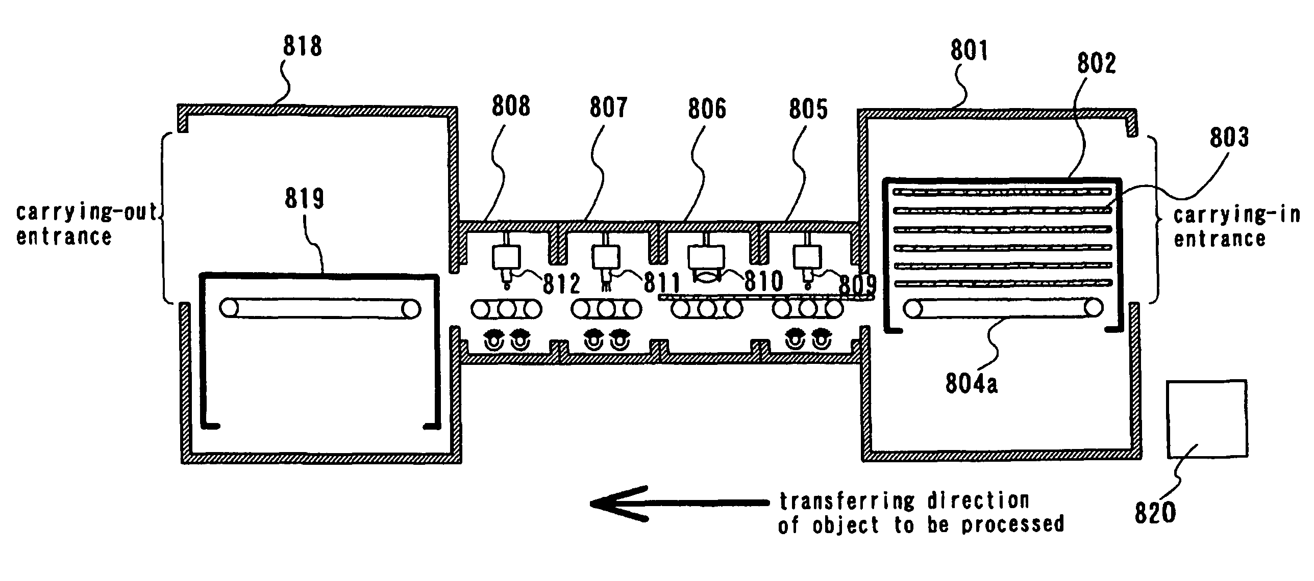
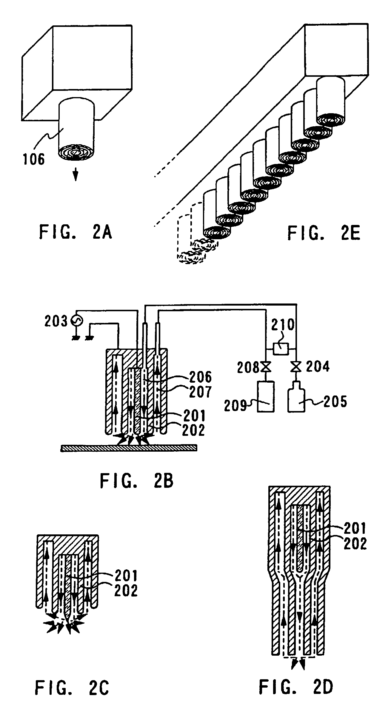
[0063]A plasma generating means 306 in the embodiment mode is a plasma generating means in which the plasma generating means 106 in the embodiment mode 1 is arranged in the intersecting direction with a transferring direction of an object to be processed 303. (FIG. 2E)

[0064]Since plurality of plasma generating means are arranged, the plasma generating means need not be moved; therefore further reduction in the processing time can be achieved.

[0065]In addition, films that are different in film qualities can be formed in the same treatment chamber by arranging plurality of plasma generating means 306 and supplying different material gases. That is, it is possible to form a silicon nitride film with a first plasma generating means, then to form a silicon oxide film w...

embodiment mode 3

[0066]This embodiment mode is an embodiment mode in which the plasma treatment apparatus in the embodiment mode 1 is applied to a dot-shaped droplet spraying apparatus. The plasma generating means is substituted for a dot-shaped droplet spraying means.

[0067]In FIG. 4, an internal structure of the droplet spraying means is described.

[0068]A droplet supplied inside a droplet spraying means 401 from the outside is moved to a nozzle portion 409 for spraying the droplet after passing a droplet chamber passage 402 and being stored in a spare droplet chamber 403. The nozzle portion constitutes a fluid resistance portion 404 provided so that a moderate droplet is charged into the nozzle, a pressurization chamber 405 for spraying the droplet outside the nozzle by applying pressure on the droplet, and a droplet spraying hole 407.

[0069]On the side wall of the pressurization chamber 405, a piezoelectric element 406 having piezoelectrical effect such as lead titanate zirconate (Pb (Zr, Ti) O3) w...


PUM

PropertyMeasurementUnit
sizeaaaaaaaaaa
sizeaaaaaaaaaa
sizeaaaaaaaaaa

Abstract

Reduction in a space of a manufacturing line, improvement of efficiency, improvement of utilization efficiency of materials, additionally, reduction in the manufacturing cost is realized by applying a means for describing a wiring pattern or a resist pattern directly on a substrate, a means for locally performing a vapor phase process such as film formation or etching under atmospheric pressure or adjacent to atmospheric pressure.

Description

BACKGROUND OF THE INVENTION[0001]1. Technical Field[0002]The present invention relates to a semiconductor manufacturing apparatus which forms a wiring, a contact hole and a display device. More specifically, the invention relates to a manufacturing method of a resist pattern by a droplet spraying method (an ink-jet method and a droplet discharging method), a manufacturing method of a metal wiring pattern by a droplet spraying method (an ink-jet method and a droplet discharging method) and a semiconductor manufacturing apparatus which forms a wiring, a contact hole and display device by using either a local CVD (Chemical Vapor Deposition) method or a local etching method performed under atmospheric pressure or adjacent to atmospheric pressure. In addition, the invention relates to a semiconductor manufacturing apparatus which forms or etches a thin film.[0003]2. Background Art[0004]In recent years, attention has been paid to a large-screen television with a diagonal size of 20 inches...

Claims


Application Information

Patent Timeline
Patent Type & Authority Patents(United States)
IPC IPC(8): C23C16/00C23F1/00H01L21/306H01L21/00
CPCH01L21/67028H01L21/6715H01L21/6708H01L21/67069H01L21/67173H01L21/67155H01L21/67253
Inventor YAMAZAKI, SHUNPEI
Owner SEMICON ENERGY LAB CO LTD
Why Eureka
Eureka Blog
Learn More