Manufacturing method of semiconductor device

a manufacturing method and semiconductor technology, applied in semiconductor devices, semiconductor/solid-state device details, electrical devices, etc., can solve the problems of difficult to remove the substrate, limit the thickness of thinning a film, and the entire surface thickness of 50 m or less, so as to prevent damage and improve the throughput speed of a semiconductor devi

Inactive Publication Date: 2011-04-19
SEMICON ENERGY LAB CO LTD
View PDF16 Cites 14 Cited by
  • Summary
  • Abstract
  • Description
  • Claims
  • Application Information

AI Technical Summary

Benefits of technology

[0007]In view of the above problems, it is an object of the present invention to provide a manufacturing method of a semiconductor device where a semiconductor element is prevented from being damaged and throughput speed thereof is improved, even in a case of thinning or removing a supporting substrate after forming the semiconductor element over the supporting substrate.
[0011]Even in a case of removing a substrate over which a semiconductor element is formed, the semiconductor element is prevented from being damaged according to the present invention. Consequently, throughput speed of a semiconductor device can be improved.

Problems solved by technology

However, in a case of removing a substrate, over which a semiconductor element is formed, by grinding treatment or polishing treatment, there is a limit of thinning a film due to a limit of accuracy of a device and in-plane uniformity of polishing; therefore, it has been difficult to make the entire surface have thickness of 50 μm or less; thus, it has been difficult to remove the substrate.
In addition, when a substrate is subjected to grinding treatment and polishing treatment, a semiconductor element provided over the substrate is stressed, thereby having fear of damaging the semiconductor element.
This is because the semiconductor element is stressed more significantly as the substrate becomes thinner; therefore, it has been difficult to remove the substrate by grinding treatment or polishing treatment.
In addition, in a case of removing the substrate, over which the semiconductor element is formed, by chemical treatment, it is extremely difficult to remove only the substrate with high yields and uniformly; thus, there has been a problem that it takes up much time to perform the treatment.

Method used


Image

  • Manufacturing method of semiconductor device
  • Manufacturing method of semiconductor device
  • Manufacturing method of semiconductor device

Examples


embodiment mode 1

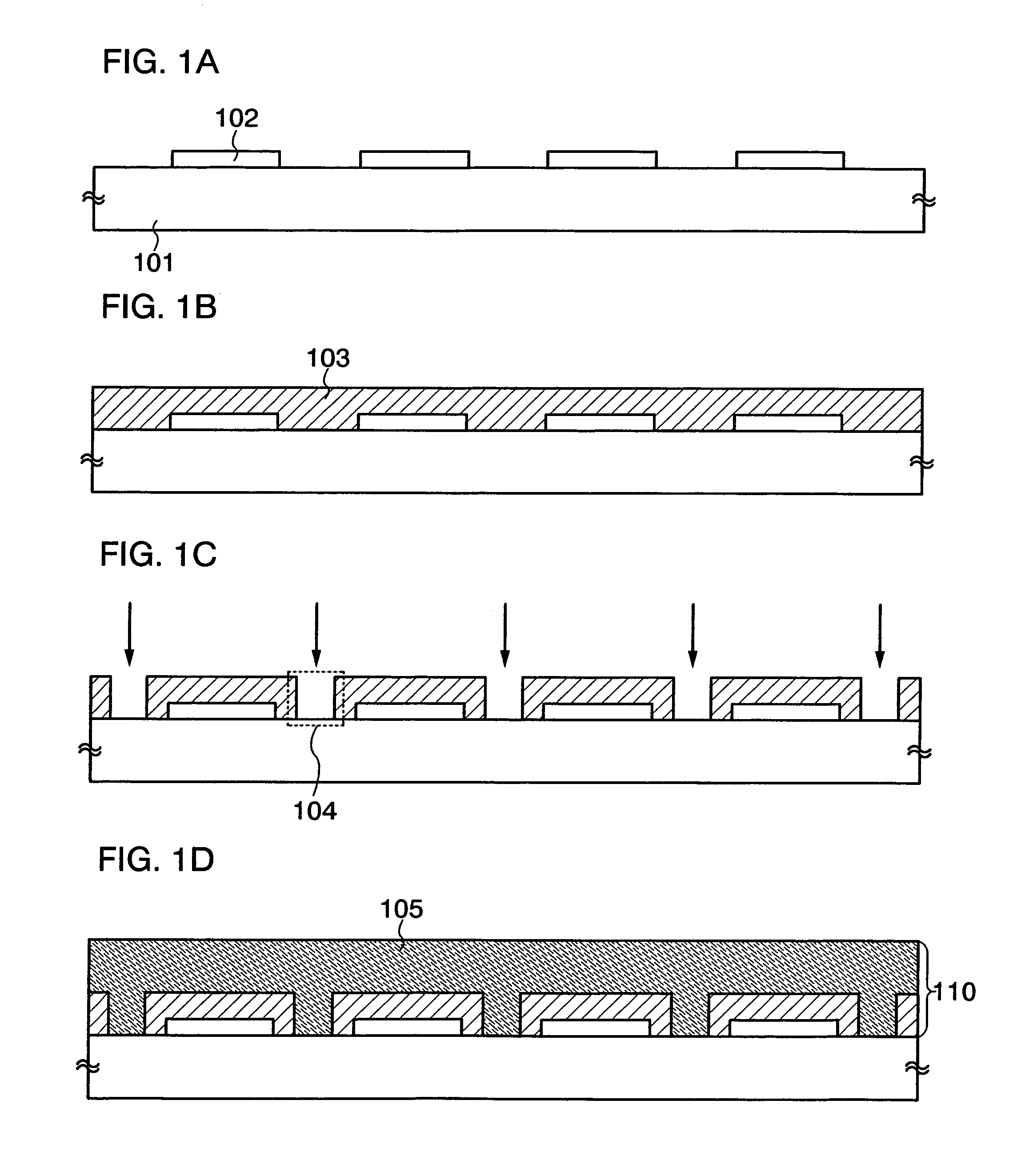
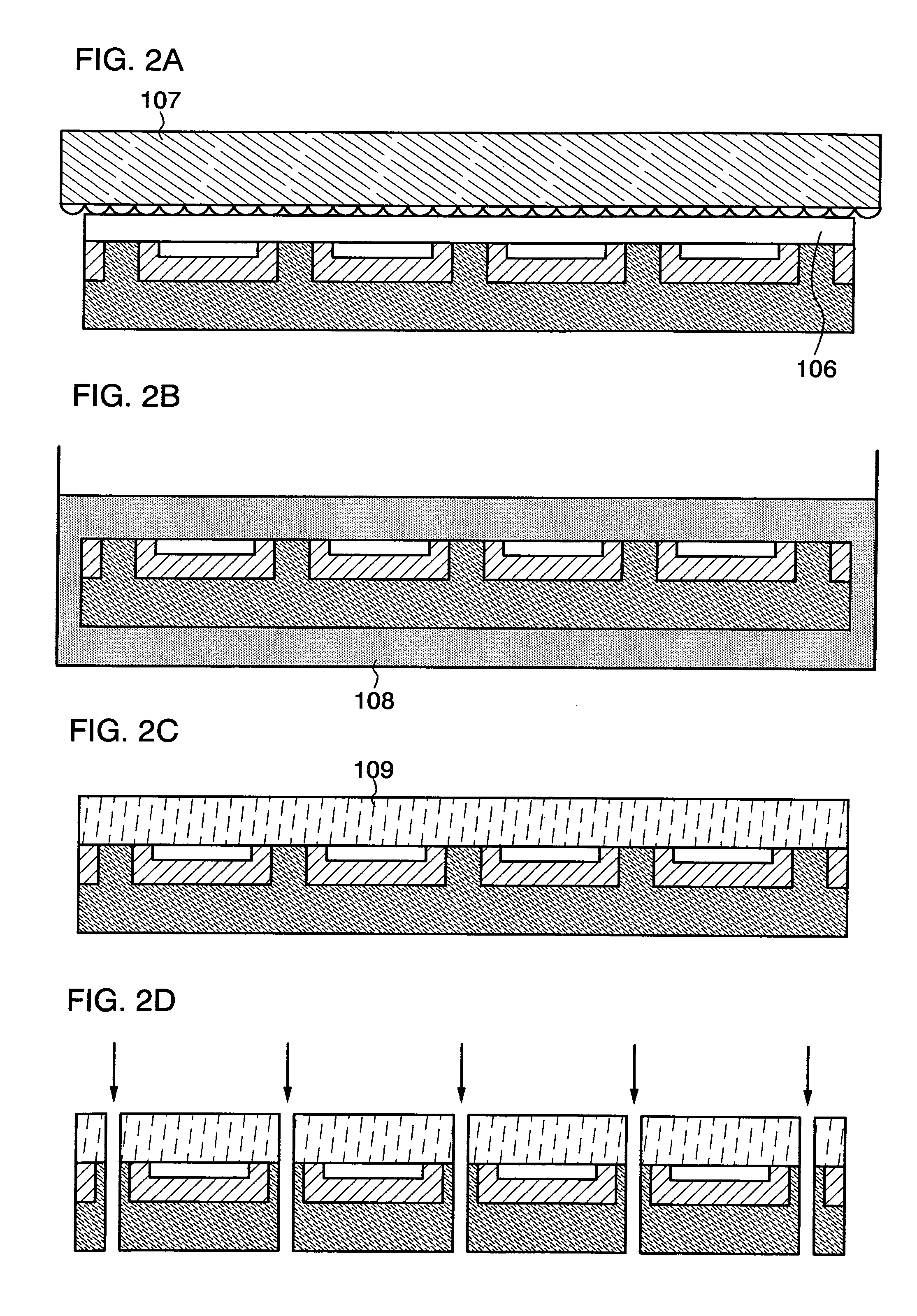
[0030]This embodiment will explain an example of a manufacturing method of a semiconductor device of the present invention with reference to drawings.

[0031]First, an element group 102 is formed over a substrate 101 (FIG. 1A). In this embodiment mode, the element group 102 constituting a semiconductor device is provided in plural over the substrate 101. By forming the element group 102 in plural over the substrate 101, a plurality of semiconductor devices can be manufactured from one substrate, which is preferable.

[0032]As the substrate 101, a glass substrate, a quartz substrate, a metal substrate or a stainless steel substrate where an insulating film is formed over one surface, a heat-resistant plastic substrate that can withstand a processing temperature in this process, or the like is preferably used. Such a substrate 101 does not have a limit in its area or shape; therefore, as long as a rectangular substrate one side of which is 1 meter or more is used as the substrate 101, for...

embodiment mode 2

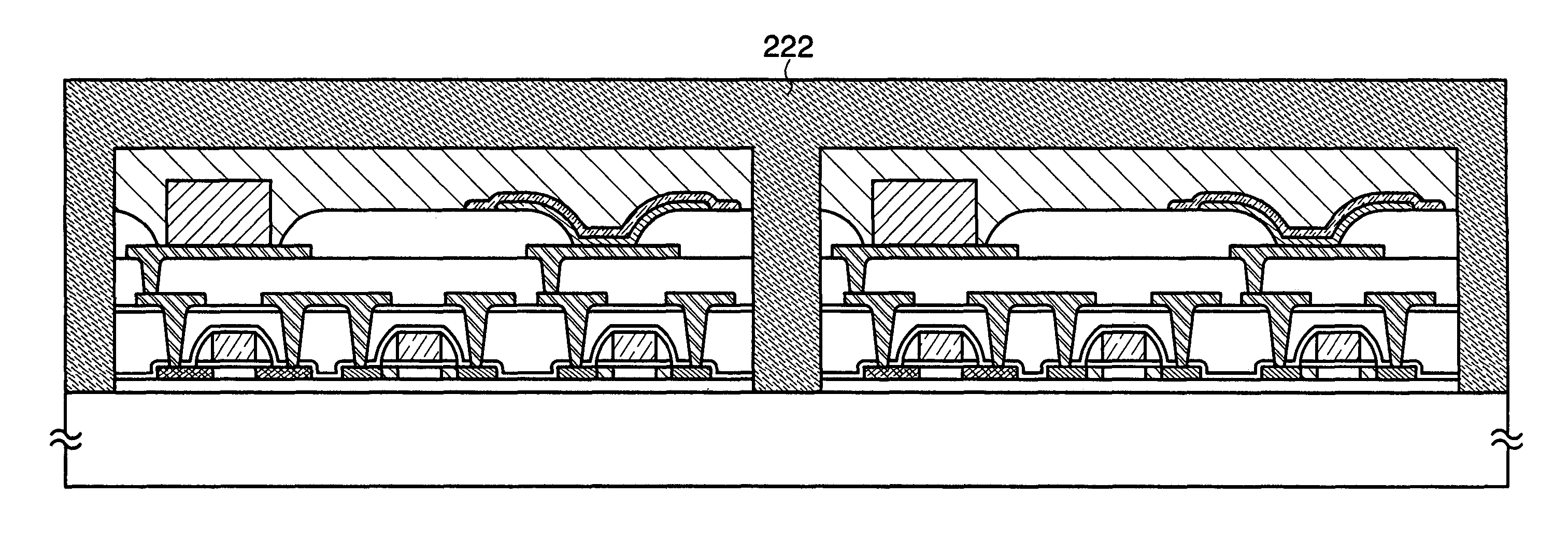
[0056]This embodiment mode will explain a manufacturing method of a semiconductor device which is different from that in the above embodiment mode with reference to drawings. Specifically, a manufacturing method of a semiconductor device of the present invention including a thin film transistor, a memory element, and an antenna will be explained with reference to drawings.

[0057]First, an insulating film 202 to be a base is formed over one surface of a substrate 201, and a semiconductor film 203 is formed over the insulating film 202 (FIG. 5A). Note that the insulating film 202 and the semiconductor film 203 can be formed continuously.

[0058]As the substrate 201, a glass substrate, a quartz substrate, a metal substrate or a stainless steel substrate where an insulating film is formed over one surface, a heat-resistant plastic substrate that can withstand a processing temperature in this process, or the like is preferably used. Such a substrate 201 does not have a limit in its area or ...

embodiment mode 3

[0113]This embodiment mode will explain an example of application modes of a semiconductor device that is obtained by using the manufacturing method described in the above embodiment mode. Specifically, applications of a semiconductor device which can exchange data without contact will be explained below with reference to drawings. The semiconductor device which can exchange data without contact is also referred to as an RFID (Radio Frequency Identification) tag, an ID tag, an IC tag, an IC chip, an RF (Radio Frequency) tag, a wireless tag, an electronic tag, or a wireless chip, depending on application modes.

[0114]A semiconductor device 80 has the function of communicating data without contact, and includes a high frequency circuit 81, a power supply circuit 82, a reset circuit 83, a clock generation circuit 84, a data demodulation circuit 85, a data modulation circuit 86, a control circuit 87 for controlling other circuits, a memory circuit 88, and an antenna 89 (FIG. 10A). The hi...


PUM


Abstract

It is an object of the present invention to provide a manufacturing method of a semiconductor device where a semiconductor element is prevented from being damaged and throughput speed thereof is improved, even in a case of thinning or removing a supporting substrate after forming the semiconductor element over the supporting substrate. According to one feature of the present invention, a method for manufacturing a semiconductor device includes the steps of forming a plurality of element groups over an upper surface of a substrate; forming an insulating film so as to cover the plurality of element groups; selectively forming an opening to the insulating film which is located in a region between neighboring two element groups in the plurality of element groups to expose the substrate; forming a first film so as to cover the insulating film and the opening; exposing the element groups by removing the substrate; forming a second film so as to cover the surface of the exposed element groups; and cutting off between the plurality of element groups so as not to expose the insulating film.

Description

TECHNICAL FIELD[0001]The present invention relates to a manufacturing method of a semiconductor device, in particular, to a manufacturing method of a semiconductor device where a supporting substrate is removed after forming a semiconductor element such as transistor over the supporting substrate.BACKGROUND ART[0002]In recent years, by forming a semiconductor element over a rigid substrate such as a glass substrate, a semiconductor device has been actively developed for use in a display such as an LCD or an organic EL display, a photoelectric conversion element such as a photo sensor or a solar cell, or the like. Besides, a semiconductor device which transmits and receives data without contact (also referred to as an RFID (Radio Frequency Identification) tag, an ID tag, an IC tag, an IC chip, a wireless tag, an electronic tag, or a wireless chip) has been actively developed. In addition, recently, a flexible device such as a film-state display or a semiconductor device embedded in p...

Claims


Application Information

Patent Timeline
Patent Type & Authority Patents(United States)
IPC IPC(8): H01L27/13H01L29/786
CPCH01L27/1266H01L27/1292H01L27/1285H01L51/56H01L24/97H01L2924/14H10K71/00H01L2924/00
Inventor WATANABE, RYOSUKE
Owner SEMICON ENERGY LAB CO LTD
Why Eureka
Try Eureka