

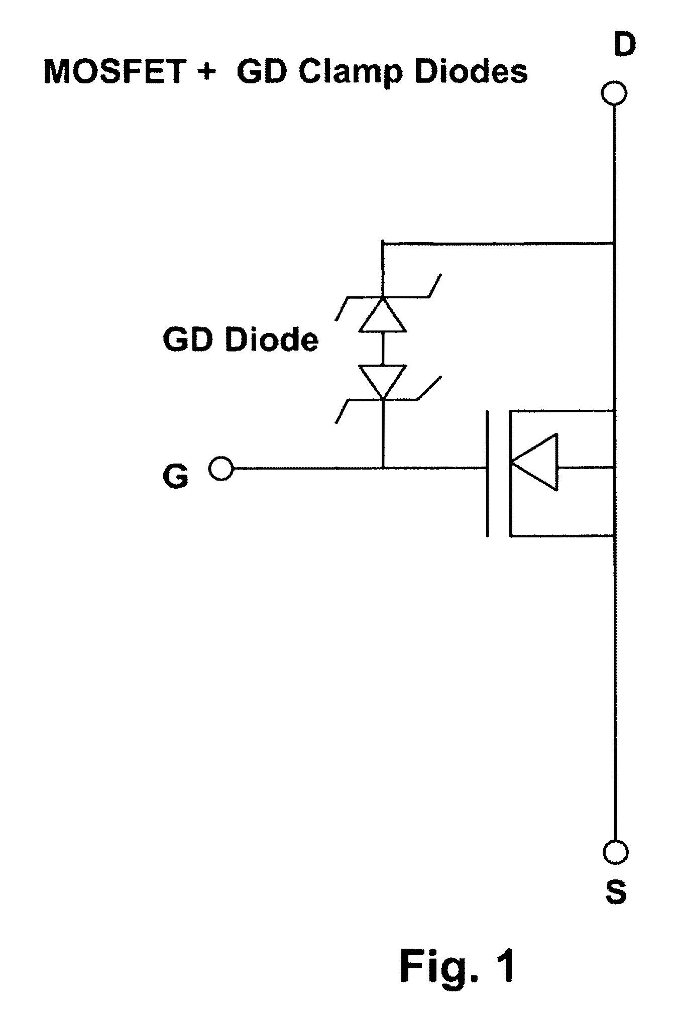
Power semiconductor devices integrated with clamp diodes having separated gate metal pads to avoid breakdown voltage degradation
a technology of power semiconductor and clamp diodes, which is applied in the direction of solid-state devices, transistors, basic electric elements, etc., can solve the problems of breakdown voltage degradation, introduction of breakdown voltage degradation of main devices, and degradation of breakdown voltage of main devices, so as to reduce contact resistance, reduce contact resistance, and reduce the effect of doping
- Summary
- Abstract
- Description
- Claims
- Application Information
AI Technical Summary
Benefits of technology
Problems solved by technology
Method used
Image

Examples
Embodiment Construction
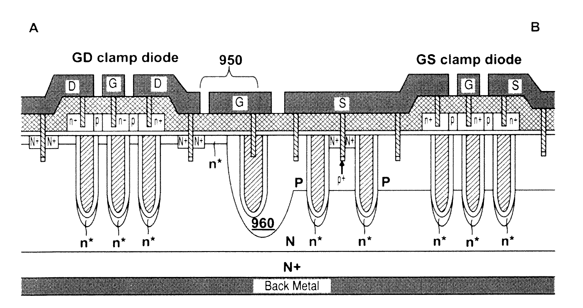
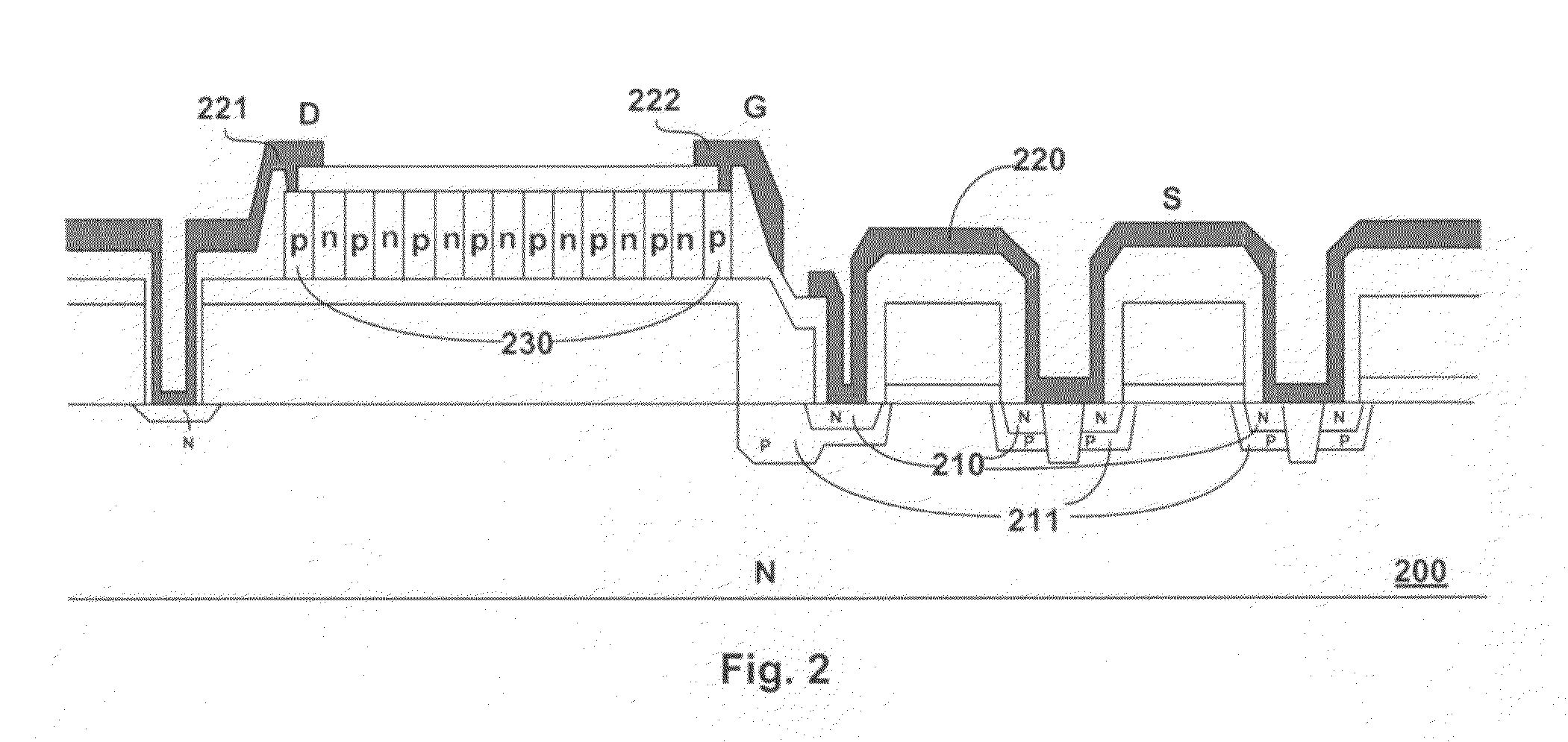
[0031]Please refer to FIG. 6 for a preferred embodiment of this invention showing the A-B cross section of FIG. 4 where a trench MOSFET device cell integrated with gate-drain and gate-source clamp diodes is formed on a heavily N+ doped substrate 600 coated with back metal 690 on rear side as drain electrode. Onto the substrate 200, a lighter N doped epitaxial layer 601 is grown, and a plurality of trenches is etched wherein. Doped poly is filled into the trenches padded with a gate insulation layer 620 formed over the inner surface of said trenches. Within these gate trenches filled with doped poly, gate trenches 611 underneath contact trenches 612 are formed to prevent shortage may caused by over etching of contact trenches 612. P-body regions 602 are extending between every adjacent trench gates 610 with N+ source region 603 near the top surface only within active area 640. Trench source-body contacts 613 filled with tungsten plug are formed penetrating through a thick oxide inter...
PUM
| Property | Measurement | Unit |
|---|---|---|
| conductivity | aaaaa | aaaaa |
| resistivity | aaaaa | aaaaa |
| conductivity type | aaaaa | aaaaa |
Abstract
Description
Claims
Application Information