Method and apparatus for automatic orientation optimization

a technology of automatic orientation and optimization, applied in the field of integrated circuit fabrication, can solve the problems of loss of structured placement requirements, affecting still suffering from manual effort for regular placement, so as to improve the timing of the entire circuit, improve the utilization rate, and improve the effect of congestion

Active Publication Date: 2011-05-03
SYNOPSYS INC
View PDF17 Cites 24 Cited by
  • Summary
  • Abstract
  • Description
  • Claims
  • Application Information

AI Technical Summary

Benefits of technology

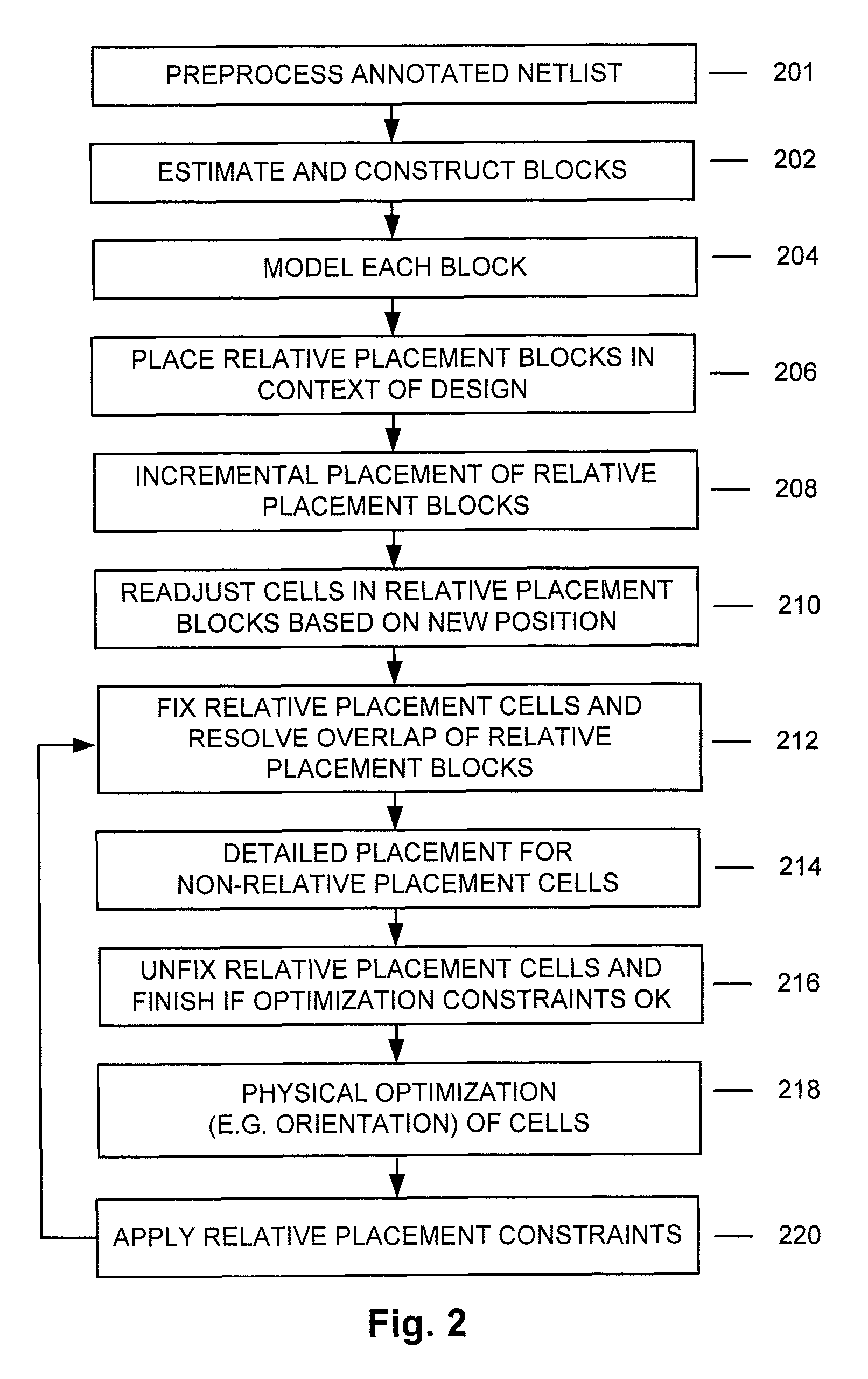
[0013]One embodiment is a method of circuit design that generates a placed, routed, and optimized circuit design. Placing and routing is performed for a netlist of a circuit design which includes a set of circuit elements. The set of circuit elements can include, for example, a register, at least part of a datapath of the circuit design, and / or a library element. Optimizing is also performed for at least part of the set of circuit elements, and generally maintains the functionality while improving the circuit design (e.g., timing, size, congestion, wire length, via counts, static power and leakage power). Such optimizing contrasts with other approaches that treat the structured placement portion of a circuit design as an immovable and otherwise unchangeable black box during routing and placement. Some examples of optimizing that involving moving the set of circuit elements, include moving some of the set of circuit elements relative to other circuit elements of the set of circuit elements, and moving the set of circuit elements together to a position in the circuit design.
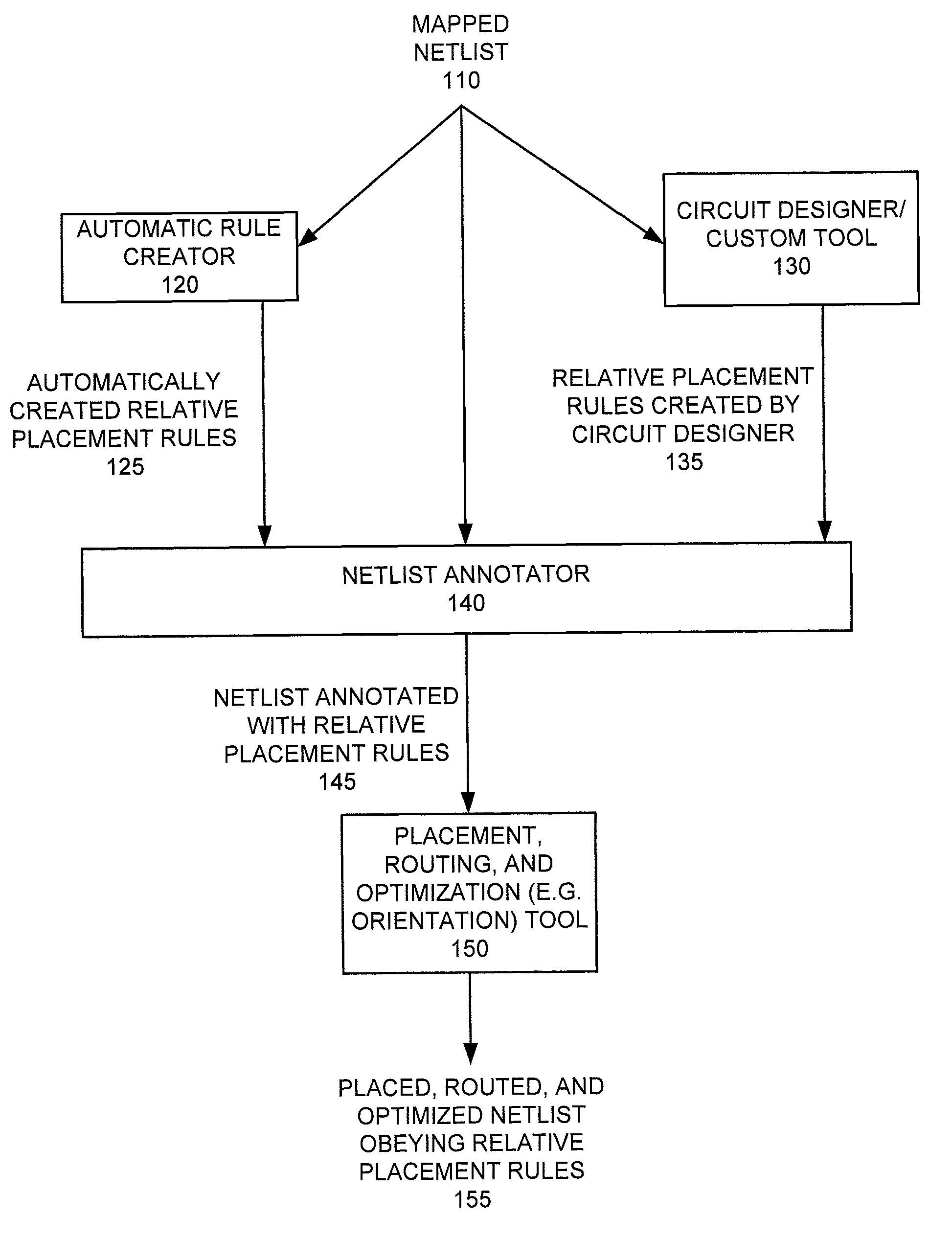
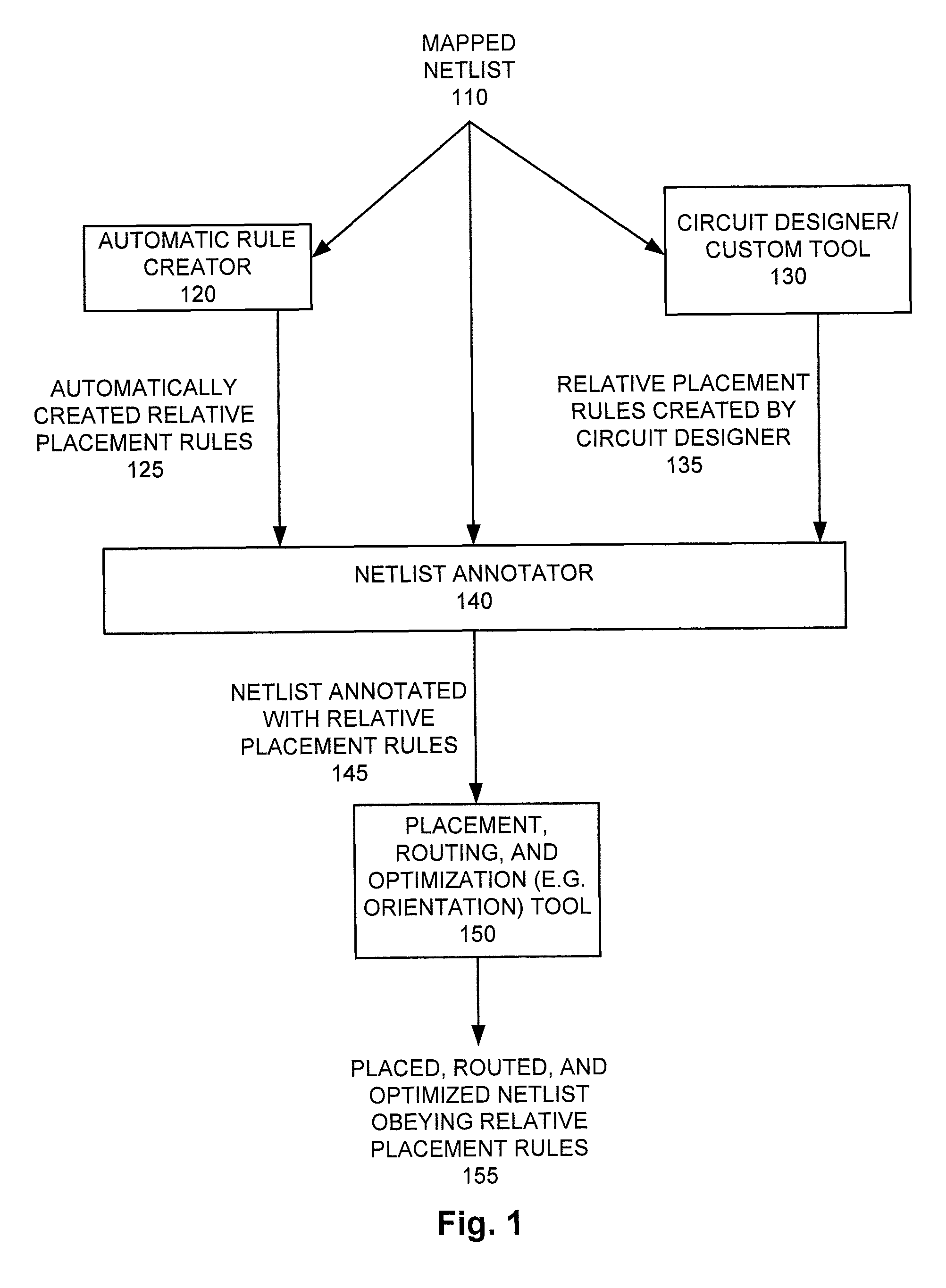
[0016]In some embodiments, these rules that specify positioning were created prior to generating the placed, routed, and optimized circuit design. The rules can be created by, for example, a human involved in creating the circuit design, or automatically by a computer analyzing the circuit design. Thus, in the event that a circuit designer feels that the judgment of a circuit designer is superior to rules generated automatically by a computer, the circuit designer can specify such rules. In contrast with other technologies where the circuit designer uses a custom tool to specify such rules, or software such as Mustang by Arcadia creates such rules, and the structured placement result is fed into a place and route tool as an immovable and otherwise unalterable black box, in such an embodiment optimization is performed on at least part of the set of circuit elements that obeys these rules in the placed, routed, and optimized circuit design. Some embodiments include creating the rules, which has the advantage of a more complete solution which combines the rule creation with the generation of the placed, routed, and optimized circuit design. In contrast, other embodiments are more limited, and generate the placed, routed, and optimized circuit design based on rules that are created outside of the embodiment. This has the advantage of being compatible with rules that area created separately from a route and place and / or optimization tool.
[0018]In some embodiments, the netlist of the circuit design further includes another set of circuit elements unconstrained by the rules. Thus, in this case, the routed, placed, and optimized circuit design includes both circuit elements that obey the rules and circuit elements that are permitted to disobey the rules. Examples of circuit elements that are unconstrained by the rules include a macro, a memory, and random logic of the circuit design. In lieu of obeying the rules, the circuit elements can, for example, be randomly placed and routed. These circuit elements can be optimized, along with the set of circuit elements affected by the rules. In contrast with other approaches that treat the structured placement portion of a circuit design as a black box while generating a routed and placed circuit design or optimizing the circuit design, in some embodiments the optimization of the set of circuit elements affected by the rules is affected by the optimization of the other set of circuit elements that are permitted to disobey the rules, and in some embodiments the optimization of the other set of circuit elements that are permitted to disobey the rules is affected by the optimization of the set of circuit elements affected by the rules. For example, if optimization of the set of elements constrained by the rules results in better congestion, then globally congestion can improve for the other set of circuit elements that are permitted to disobey the rules, resulting in better design utilization. In another example, if a timing critical path of a design runs through both the set of elements constrained by the rules and the other set of circuit elements that are permitted to disobey the rules, then to the extent that that other set of circuit elements that are permitted to disobey the rules has been optimized, optimization will be more effective on the set of elements constrained by the rules, such as by aggressively sizing them to meet timing constraints. In another example, accurate routing estimates for the set of elements constrained by the rules, when compared to the set of elements that are permitted to disobey the rules, will enable aggressive optimization for both sets of elements, thus improving timing for the entire circuit. In another example is, logic optimizations, which are aware of the rules, could reduce the area for the set of the elements constrained by the rules, thus freeing up space for the set of elements permitted to disobey the rules, allowing better timing optimizations, by choosing bigger cells.

Problems solved by technology

However, regularized placement still suffers from a great deal of manual effort, such as in cell drive strength selection.
Capturing a priori designer knowledge of structured placement requirements in HDL is a nontrivial problem.
Even if captured, structured placement requirements are lost during standard cell random placement.
This results in not just loss of regularity, but also extra buffering, routing, vias, and cell oversizing, compared to a solution which might be obtained following structured placement.
This approach is quite expensive in terms of engineering effort.
This approach is also hard to integrate with the rest of the design.
Unfortunately, this triggers another iteration, with further manual sizing and optimization efforts through the homegrown tools for the block with structured placement.
The initial structure generated through synthesis or through the special tool is problematic.
Because the initial structure is generated prior to placement, the initial structure is formed lacking complete placement knowledge, and thus the initial structure fails to lead to optimal placement as generation.
Also if it is passed as a macro / IP block, then place and route tools cannot resize or otherwise optimize the blocks.
Although circuit design parameters such as wiring congestion, wiring alignment, wire crossing, and wire length would be improved by finding the ideal orientation of all cells, this has been a computationally intractable problem.
Because the number of possible orientations explodes combinatorially for the number of cells of practical commercial designs, finding the ideal orientation of all cells has remained an intractable problem.
In some circumstances, the placed, routed, and optimized circuit design will not be desirable.
For example, the rules specifying position may be less than ideal and require tweaking or more drastic revision, or the circuit design itself may require modification, such as the rearrangement of circuit elements, or addition or deletion of circuit elements.

Method used


Image

  • Method and apparatus for automatic orientation optimization
  • Method and apparatus for automatic orientation optimization
  • Method and apparatus for automatic orientation optimization

Examples


example

[0309]To save all the relative placement groups to disk, remove the information from the design, then recreate the information on the design, enter

[0310]

psyn_shell-xg-t> find rp_group{mul::grp_mul ripple::grp_ripple example3::top_group}psyn_shell-xg-t> write_rp_group -all -output my_groups.tcl1psyn_shell-xg-t> remove_rp_group -all -quiet1psyn_shell-xg-t> find rp_groupError: Can't find objects matching ’*’. (UID-109)psyn_shell-xg-t> source my_groups.tcl{example3::top_group}psyn_shell-xg-t> find rp_group{example3::top_group ripple::grp_ripple mul::grp_mul}

[0311]Aligning Relative Placement by Pins

[0312]Columns can be aligned by pins instead of by the lower-left corner (the default). This capability increases the probability of straight routes and can result in less congestion, lower power, and lower routing resources by eliminating vias.

[0313]To align a group by pins, use the create_rp_group command with its—pin_align_name switch.

[0314]When aligning by pins, one or more of the followin...


PUM


Abstract

Methods and apparatuses are disclosed for automatic orientation optimization in the course of generating a placed, routed, and optimized circuit design. Also disclosed are a circuit design and circuit created with the technology. Also disclosed are a circuit design and circuit created with the technology.

Description

REFERENCE TO RELATED APPLICATIONS[0001]This application claims the benefit of U.S. Provisional Application No. 61 / 025,263 filed 31 Jan. 2008, which application is incorporated herein by reference.BACKGROUND[0002]1. Field[0003]The technology relates to integrated circuit fabrication, and more particularly to placement, routing, and optimization of an integrated circuit design that obeys rules that specify the relative placement of circuit elements.[0004]2. Description of Related Art[0005]An integrated circuit design flow typically proceeds through the following stages: product idea, EDA software, tapeout, fabrication equipment, packing / assembly, and chips. The EDA software stage includes the steps shown in the following table:[0006]EDA stepWhat HappensSystem DesignDescribe the functionality to implementWhat-if planningHardware / software architecture partitioningLogic Design andWrite VHDL / Verilog for modules in systemFunctionalCheck design for functional accuracy, does the design produ...

Claims


Application Information

Patent Timeline
Patent Type & Authority Patents(United States)
IPC IPC(8): G06F17/50
CPCG06F17/5072G06F17/5081G06F17/5077G06F30/394G06F30/392G06F30/398
Inventor ARUNACHALAM, ANANDIYER, MAHESH ANANTHARAMAN
Owner SYNOPSYS INC
Why Eureka
Try Eureka