Electromagnetic wave absorption board to be used in wireless LAN
a technology of electromagnetic waves and absorption boards, which is applied in the direction of parallel plane units, instruments, and reradiation, etc., can solve the problems of electromagnetic noise in buildings, intrusion of transmission into buildings inside, and electromagnetic waves emitted by devices used
- Summary
- Abstract
- Description
- Claims
- Application Information
AI Technical Summary
Benefits of technology
Problems solved by technology
Method used
Image
Examples
example 1
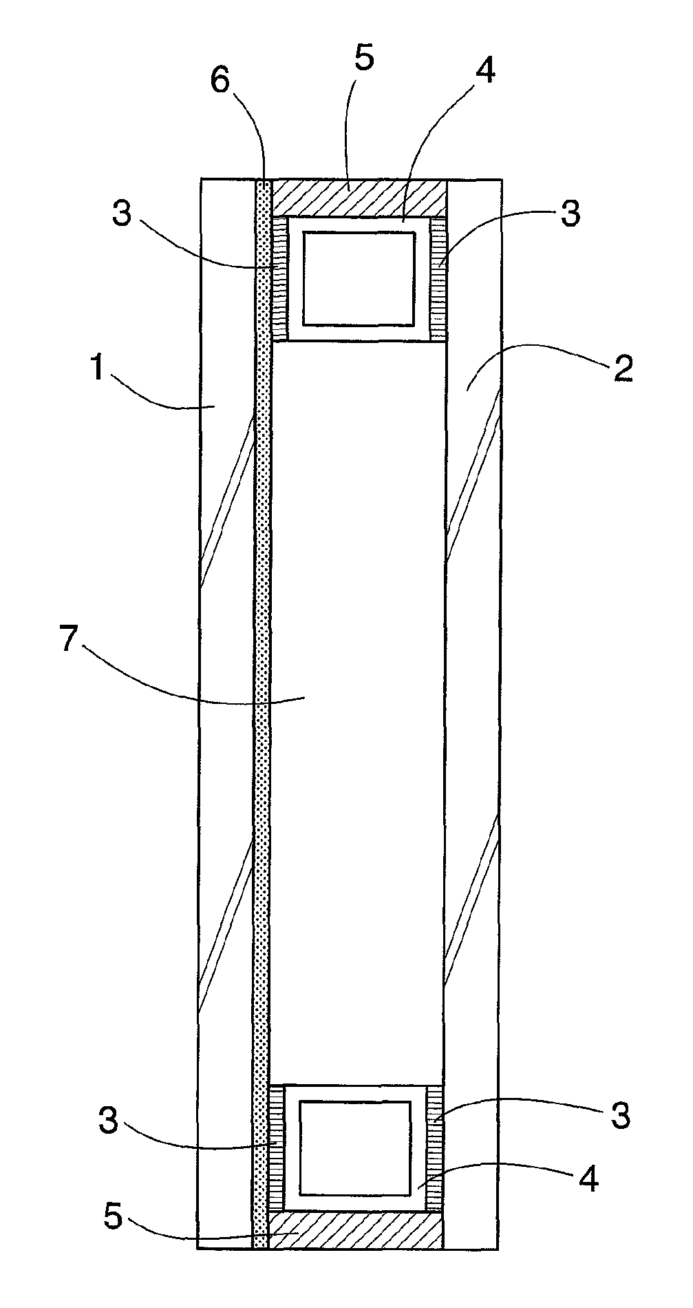
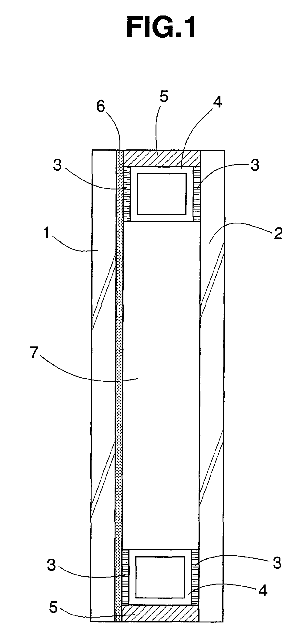
[0131]As an electromagnetic absorption board of a structure shown in FIG. 1, Samples 1-4 were prepared, which were different in thickness of the glass sheet, thickness of the hollow layer 7 and surface resistivity value of the resistive film, as shown in Table 7, by using float-produced glass sheets for the dielectrics 1, 2. The hollow layer 7 was filled with air. As the spacer, there was used a spacer having a hollow rectangular sectional shape and made of aluminum. The distance of the hollow layer was changed by the size of the spacer.
[0132]Samples 1-4 are electromagnetic wave absorption boards prepared to be used for 2.45 GHz frequency band of wireless LAN in the case of Case 1.
[0133]As the resistive film, one prepared by forming TiO2 film, Cr film and SnO2 film in this order by sputtering method was used. Surface resistivity of the resistive film was adjusted by the film thickness.
[0134]Electromagnetic wave absorption capability of the electromagnetic wave absorption boards (Sam...
example 2
[0144]Similar to Example 1, electromagnetic wave absorption boards (Samples 5-8) shown in Table 8 were prepared to be used in 5.2 GHz frequency band of wireless LAN in the case of Case 1. Furthermore, similar to Example 1, the amount of absorption of electromagnetic wave was measured.
[0145]In Table 8, the amounts of absorption of electromagnetic wave determined by calculation and the measured amounts of electromagnetic wave are shown, both values well coincided.
[0146]
TABLE 8SampleSampleSampleSample5678Structure ofThickness of Glass Sheet6666ElectromagneticWith Resistive Film (mm)Wave AbsorptionThickness of Glass Sheet3333BoardOpposingly Disposed (mm)Thickness of Air Layer (mm)612612Surface Resistivity Value of Resistive Film (Ω / □)57573030Amount of(Calculated Value dB)20211010Electromagnetic(Measured Value dB)20211015Wave Absorption
example 3
[0147]Electromagnetic wave absorption boards (Samples 9-11) shown in Table 9 were prepared to be used in 2.45 GHz frequency band of wireless LAN in the case of Case 2 by repeating Example 1 except in that a resistive film was prepared by forming ZnO2 film, Al film and ZnO2 film in this order by sputtering method.
[0148]Similar to Example 1, the amount of absorption of electromagnetic wave was measured. In Table 9, the amounts of absorption of electromagnetic wave determined by calculation and the measured amounts of absorption of electromagnetic wave are shown, and both values well coincided.
[0149]
TABLE 9Sample 9Sample 10Sample 11Structure ofThickness of Glass Sheet12610ElectromagneticOpposingly Disposed (mm)Wave AbsorptionThickness of Glass Sheet646BoardWith Resistive Film (mm)Thickness of Air Layer (mm)61212Surface Resistivity Value of Resistive Film (Ω / □)100240120Amount of(Calculated Value dB)303010Electromagnetic(Measured Value dB)303010Wave Absorption
PUM
| Property | Measurement | Unit |
|---|---|---|
| thickness | aaaaa | aaaaa |
| thickness | aaaaa | aaaaa |
| thickness | aaaaa | aaaaa |
Abstract
Description
Claims
Application Information


