Semiconductor device

a technology of semiconductors and devices, applied in the direction of digital storage, pulse automatic control, instruments, etc., can solve the problems of sudden increase of current consumption, easy reduction of internal voltage and external voltage, and inability to induce read operation errors

Inactive Publication Date: 2011-05-31
SK HYNIX INC
View PDF26 Cites 4 Cited by
  • Summary
  • Abstract
  • Description
  • Claims
  • Application Information

AI Technical Summary

Benefits of technology

[0005]Embodiments of the present invention are directed to a semiconductor device, and more particularly, to a semiconductor device providing a reliable data valid window.

Problems solved by technology

However, the voltage levels of the internal voltage and the external voltage are easily decreased in a practical read operation of the semiconductor device because of the abrupt current consumption.
Due to the abovementioned decrease of the internal voltage, a read operation error can be induced.
In the operation of the internal circuits, the current consumption is abruptly increased.
As a result, an initial data valid window becomes relatively narrow because of the abrupt current consumption and the semiconductor device fails to perform an initial read operation correctly.

Method used


Image

  • Semiconductor device
  • Semiconductor device
  • Semiconductor device

Examples


Embodiment Construction

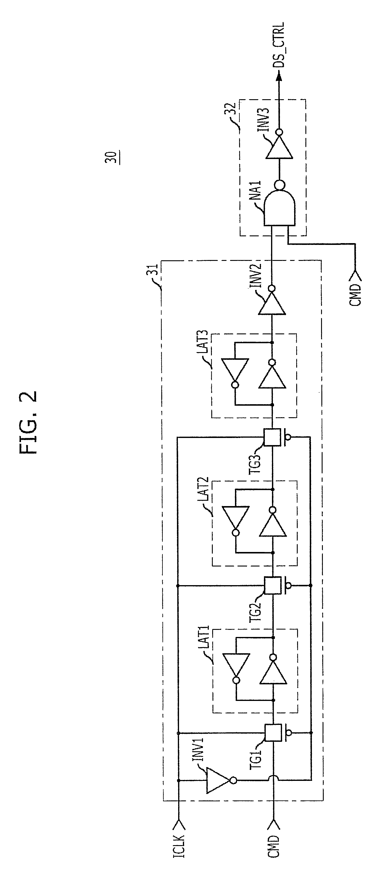
/ b>FIG. 3 is a detailed circuit diagram of the clock driver in accordance with an embodiment of the present invention.

[0012]FIG. 4 is a detailed circuit diagram of the clock driver in accordance with another embodiment of the present invention.

DESCRIPTION OF SPECIFIC EMBODIMENTS

[0013]Other objects and advantages of the present invention can be understood by the following description, and become apparent with reference to the embodiments of the present invention.

[0014]Hereinafter, a semiconductor device securing a reliable data process in accordance with an embodiment of the present invention will be described in detail.

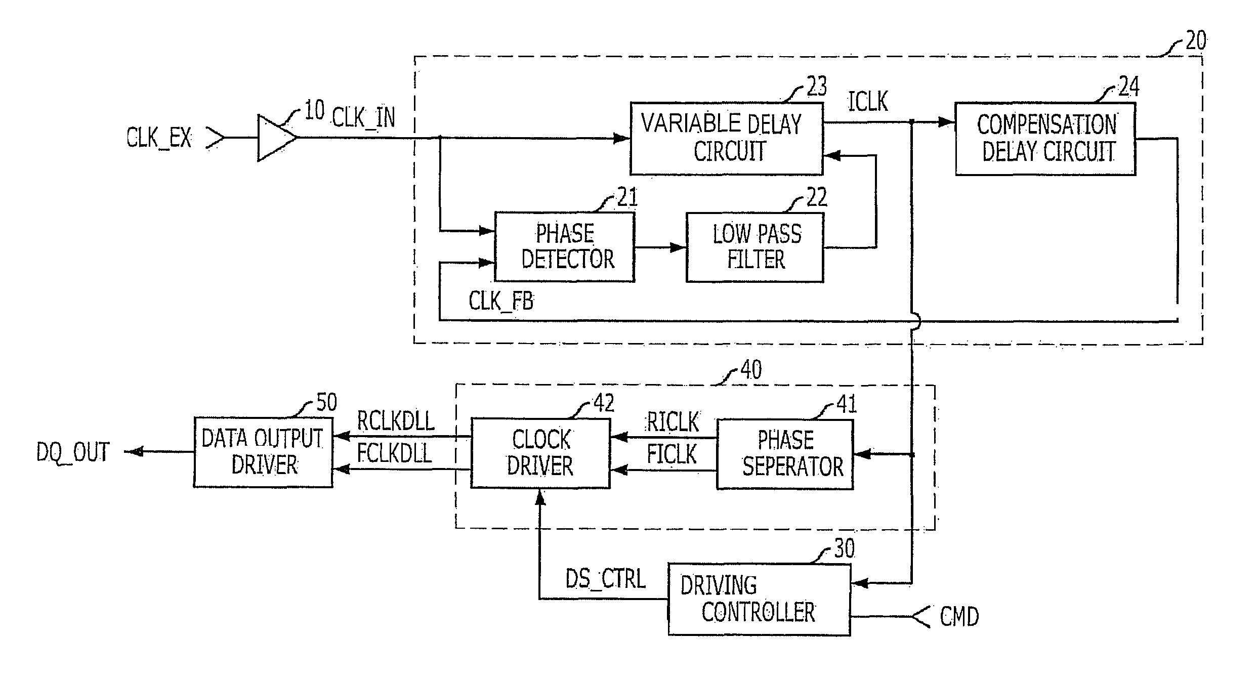
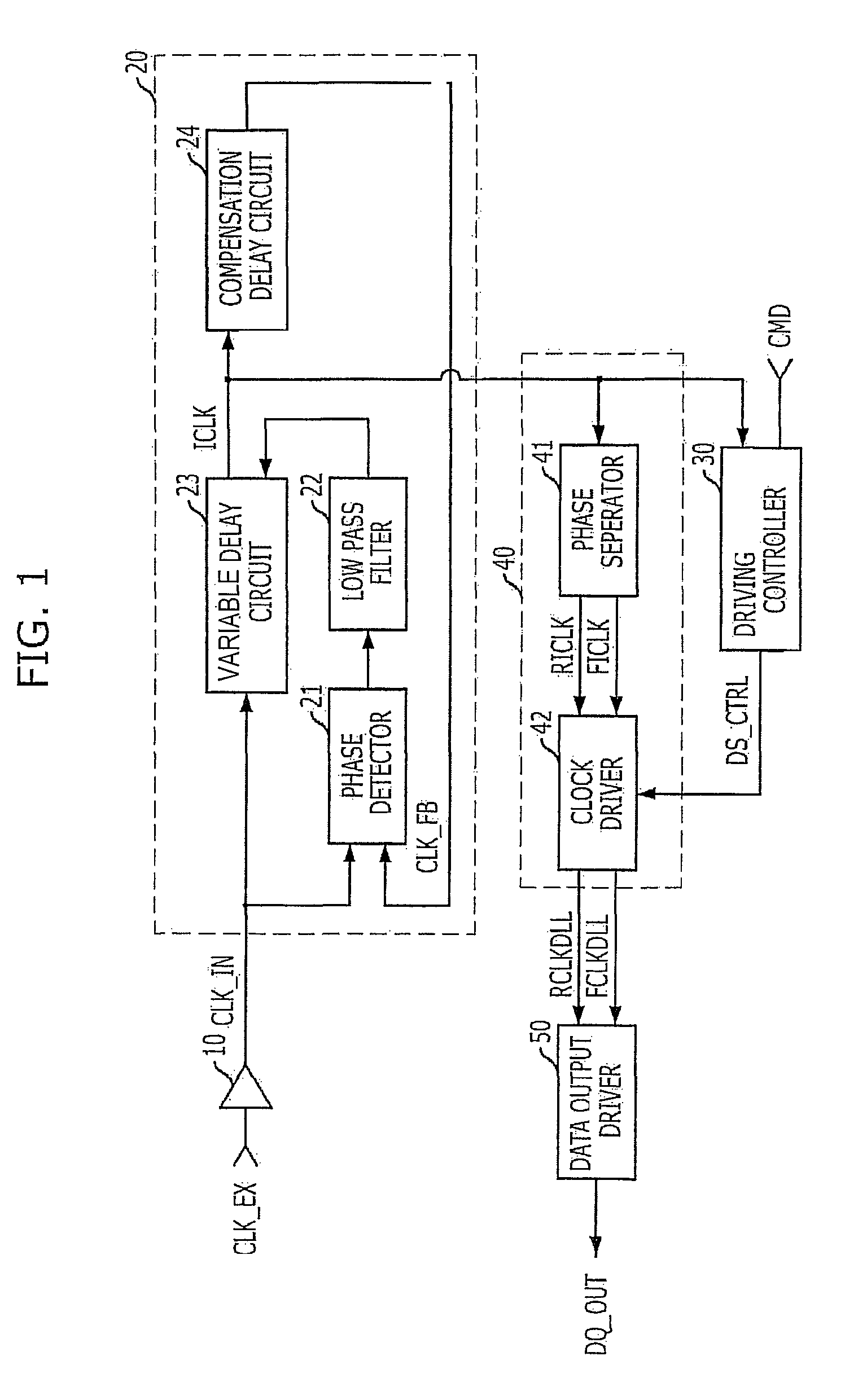
[0015]FIG. 1 is a block diagram illustrating a semiconductor device in accordance with an embodiment of the present invention.

[0016]Referring to FIG. 1, the semiconductor device includes a clock buffer 10, a delay-locked loop (DLL) circuit 20, a driving controller 30, a DLL driver 40, and a data output driver 50. The clock buffer 10 generates an input clock CLK_IN by ...


PUM


Abstract

A semiconductor device for providing a reliable data valid window includes a drive control unit configured to output a driving power control signal in response to an internal clock and a command signal; a sub-drive voltage supply unit configured to supply sub-drive voltages; a main drive unit configured to generate a delay-locked loop (DLL) clock by driving the internal clock with a main drive voltage; a sub-drive unit configured to drive the internal clock with the sub-drive voltage in response to the driving power control signal; and a data output driver configured to drive and output a data signal in sync with the DLL clock, wherein the main drive unit and the sub-drive unit share their output terminal.

Description

CROSS-REFERENCE TO RELATED APPLICATION[0001]The present invention claims priority of Korean patent application number 10-2008-0108050, filed on Oct. 31, 2008, which is incorporated by reference in its entirety.BACKGROUND OF THE INVENTION[0002]The present invention relates to a semiconductor device, and more particularly, to a semiconductor device providing a reliable data valid window.[0003]A semiconductor memory device generates an internal voltage having a stable voltage level by using an external voltage supplied from an external circuit in order to perform a reliable operation. However, the voltage levels of the internal voltage and the external voltage are easily decreased in a practical read operation of the semiconductor device because of the abrupt current consumption. Due to the abovementioned decrease of the internal voltage, a read operation error can be induced.[0004]In detail, several internal circuits, e.g., a sense amplifier, a pre-driver, and an output driver, which ...

Claims


Application Information

Patent Timeline
Patent Type & Authority Patents(United States)
IPC IPC(8): H03L7/06
CPCH03L7/0812H03L7/0816G11C5/147G11C7/1066G11C7/22H03K5/13
Inventor LEE, SEONG-JUN
Owner SK HYNIX INC
Why Eureka
Try Eureka