Apparatus and method for reducing interference

a technology of interference reduction and circuit, applied in semiconductor/solid-state device testing/measurement, semiconductor/solid-state device details, instruments, etc., can solve problems such as difficult system design, circuit interference of inductors, and interference of other components of circuits, so as to reduce interference in circuits, minimize interference, and maximize magnetic cancellation

Active Publication Date: 2011-06-07
SILICON LAB INC
View PDF12 Cites 3 Cited by
  • Summary
  • Abstract
  • Description
  • Claims
  • Application Information

AI Technical Summary

Benefits of technology

[0005]Another embodiment of the invention provides a method of reducing interference in a circuit including forming an inductance using two or more inductors, with the inductors arranged such that current flows through the inductors in different directions to at least partially cancel magnetic fields generated from the inductors.
[0006]Another embodiment of the invention provides a method of minimizing interference between circuitry on an integrated circuit, including forming an inductance on the integrated circuit using to or more conductive loops coupled together. In one example, the conductive loops define a first axis extending through the conductive loops and a second axis perpendicular to the first axis. In this example, the method includes configuring the conductive loops such that current flows in opposite directions through some of the loops to at least partially cancel magnetic fields generated from the loops, and such that magnetic cancellation is maximized at locations along the second axis. The relative positions circuitry is configured to achieve a desired amount of magnetic cancellation.

Problems solved by technology

In various types of circuits, interference can cause problems with the operation of circuits.
Interference can therefore make the design of a system difficult.
For example, in a circuit where inductors are used, the inductors can interfere with other components in the circuit.
This type of integration can be difficult and involves solving several problems.

Method used


Image

  • Apparatus and method for reducing interference
  • Apparatus and method for reducing interference
  • Apparatus and method for reducing interference

Examples


Embodiment Construction

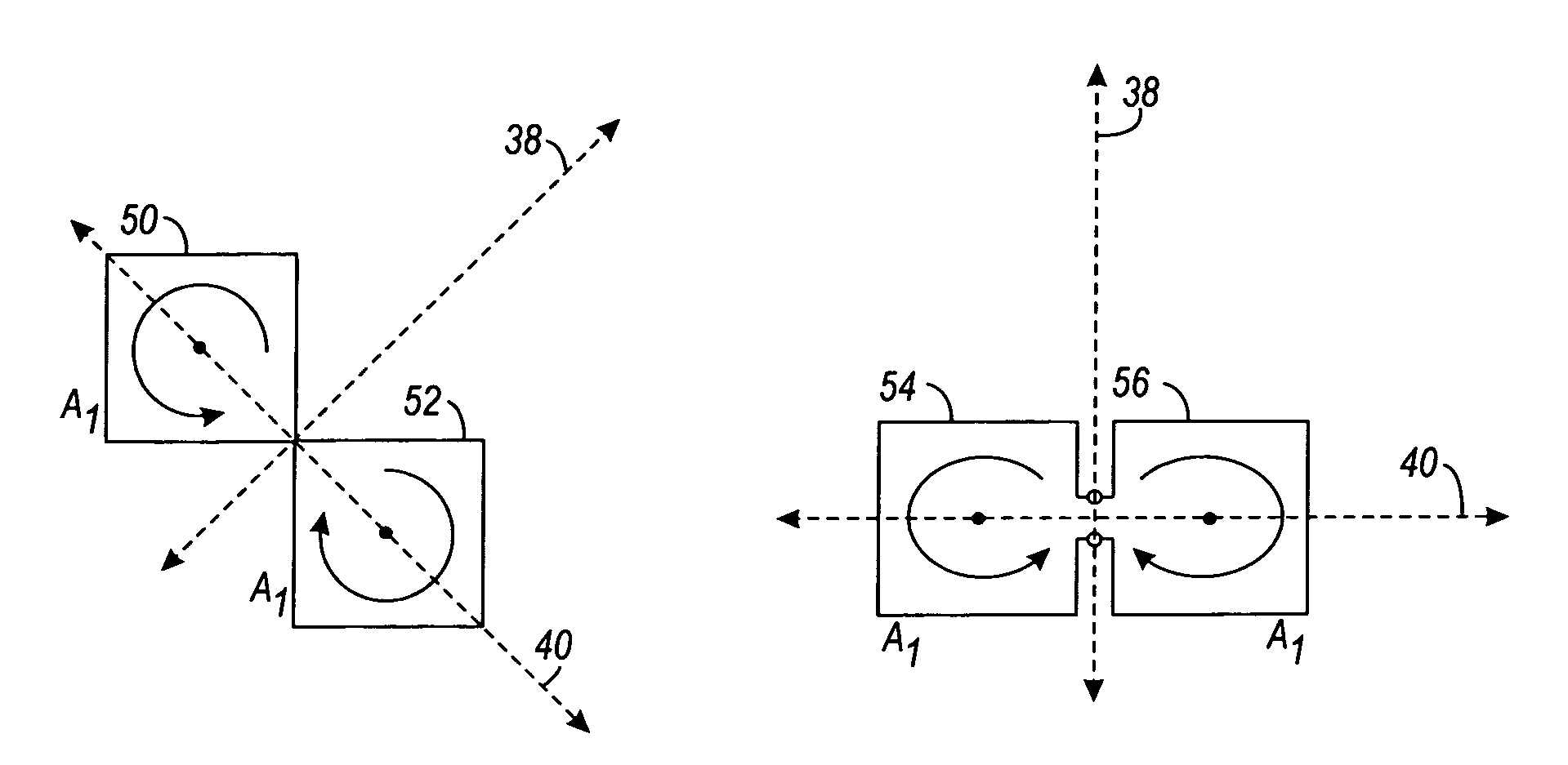
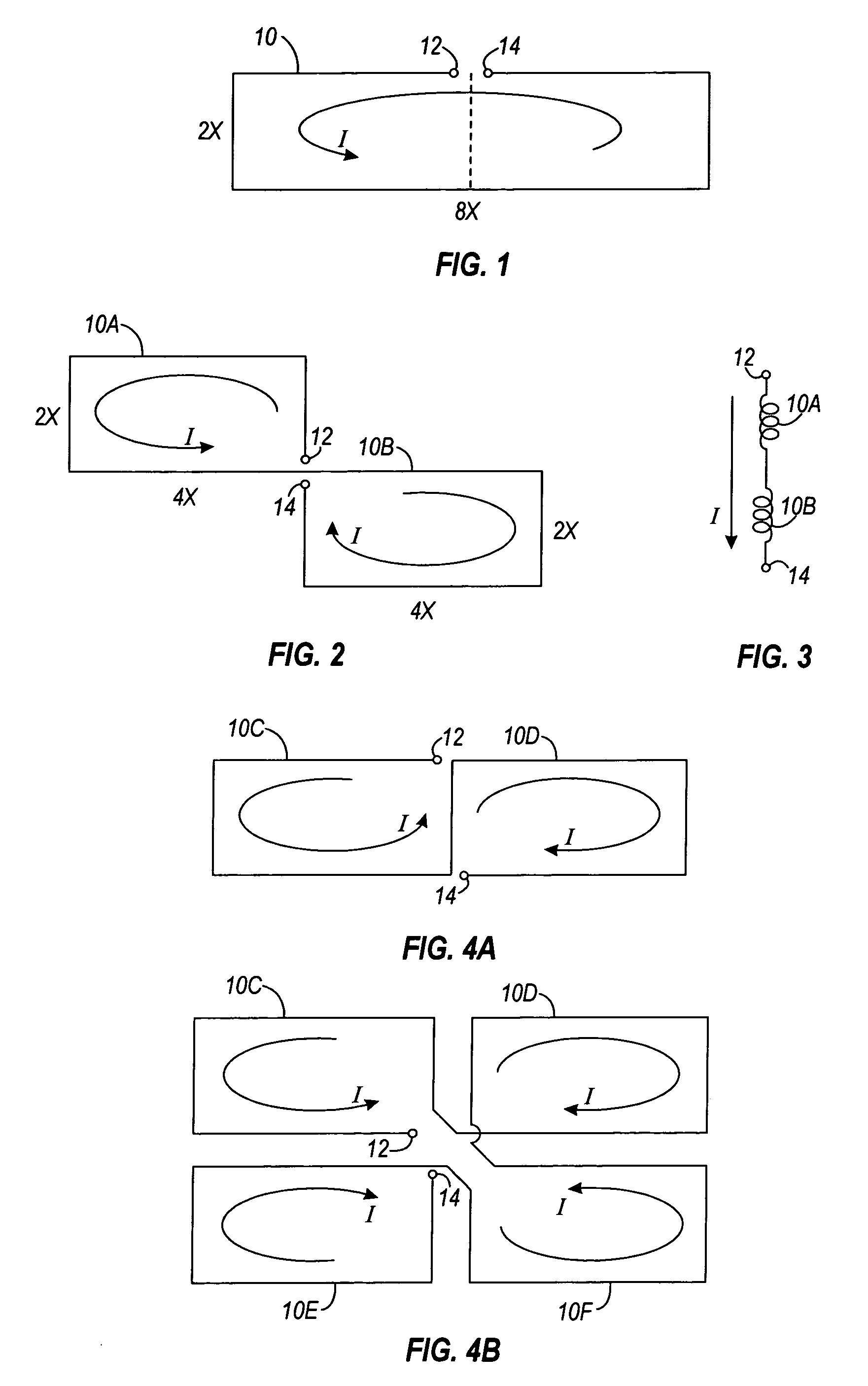
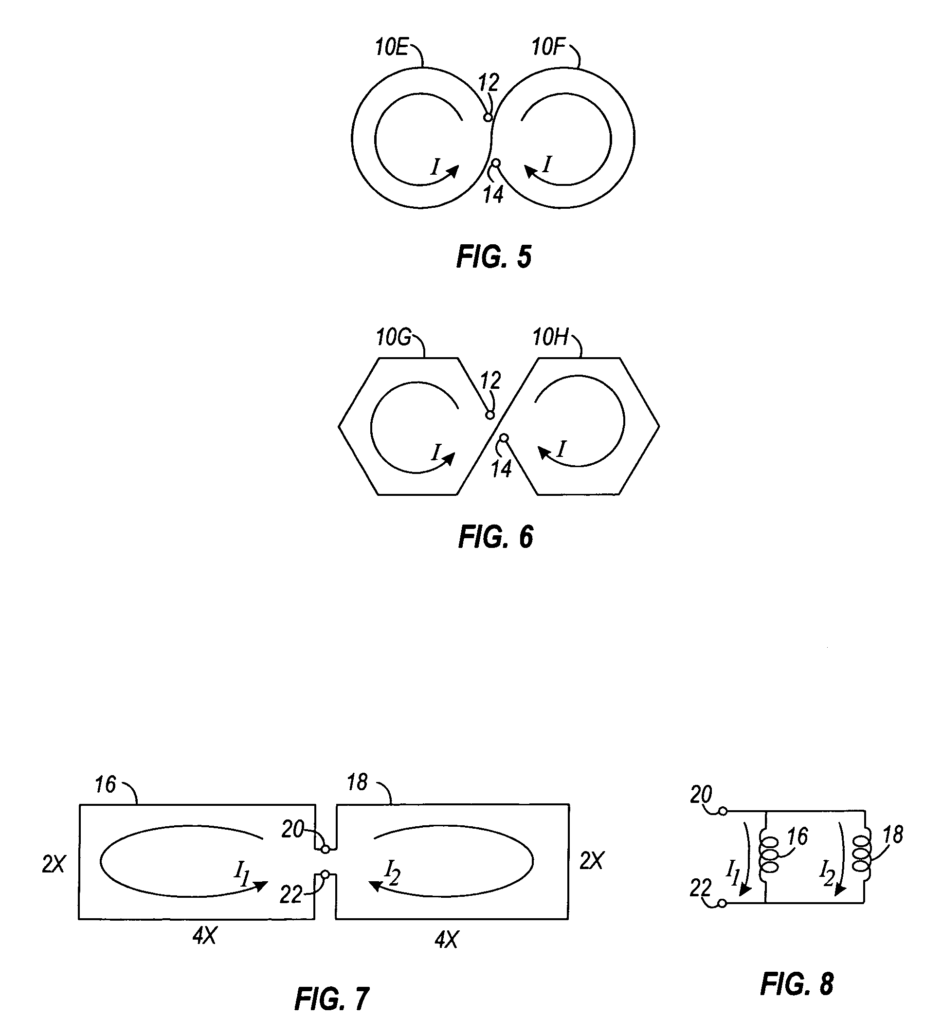
[0026]An IC utilizing techniques of the present invention may be used for any desired application, including wireless transmission systems such as mobile or cellular communication devices or other wireless devices. Note, however, that the present invention may be used in any other application where it is desirable to reduce or minimize interference in a circuit formed on a printed circuit board, an IC, or any other type of package.

[0027]In order to provide a context for understanding this description, the following description illustrates one example of a typical application of the present invention. Techniques may be used to help provide a highly integrated, low cost, low form-factor RF apparatus, while also satisfying the requirements of any applicable standards that govern the performance of the RF apparatus. In one example, an RF apparatus takes the form of an RF receiver or transceiver for a high performance communication system. Such an apparatus may include various blocks of ...


PUM


Abstract

A method and apparatus is provided for use in an integrated circuit or printed circuit board for reducing or minimizing interference. An inductance is formed using two or more inductors coupled together and configured such that current flows through the inductors in different directions, thus at least partially canceling magnetic fields. When designing a circuit, the configuration of the inductors, as well as the relative positions of portions of the circuit, can be tweaked to provide optimal interference or noise control.

Description

FIELD OF THE INVENTION[0001]This patent document relates generally to techniques for reducing interference in a circuit, and more particularly to techniques using magnetically differential inductors to reduce interference in a circuit.BACKGROUND OF THE INVENTION[0002]In various types of circuits, interference can cause problems with the operation of circuits. Interference can therefore make the design of a system difficult. For example, in a circuit where inductors are used, the inductors can interfere with other components in the circuit.[0003]In the example of mobile radio and telephony applications, demand for smaller and lower cost devices has driven recent research toward the integration of components into single IC's. For example, efforts have been made to integrate radio-frequency (RF) transceivers within a single IC, using technologies such as complementary metal-oxide semiconductor (CMOS) technologies. This type of integration can be difficult and involves solving several p...

Claims


Application Information

Patent Timeline
Patent Type & Authority Patents(United States)
IPC IPC(8): H01L21/00H01L27/08H01L29/82
CPCH01F17/0006H04R3/00H01F27/346H01F2017/0073
Inventor MARQUES, AUGUSTO MANUEL
Owner SILICON LAB INC
Why Eureka
Try Eureka