Supercharge Your Innovation With Domain-Expert AI Agents!

Flash memory cell string

a flash memory and cell technology, applied in the field of flash memory cell strings, can solve the problems of large difficulty, large size of cells, and u-shape structure of existing structures, and achieve the effect of excellent size reduction characteristics and excellent performan

Active Publication Date: 2011-06-14
SEOUL NAT UNIV R&DB FOUND
View PDF3 Cites 5 Cited by
  • Summary
  • Abstract
  • Description
  • Claims
  • Application Information

AI Technical Summary

Benefits of technology

The solution effectively suppresses short-channel effects, increases read current, and improves size reduction characteristics, enabling higher integration and performance without the need for source / drain regions, thus enhancing the overall performance and capacity of NAND flash memory devices.

Problems solved by technology

103, 2006), which realizes a high coupling effect and low crosstalk using existing floating gates, was published by the Samsung Electronics Co. Ltd. However, with the reduction in the size of cells, in order to form a U-shape floating-poly electrode, the pitch of the poly electrode in the direction of channel width increases to about 100 nm or more, thus causing problems.
Further, with the reduction in the size of cells, a U-shape structure and an existing structure exhibit a serious short-channel effect at a gate length of about 45 nm or less.
Further, demands for a multi-level cell have increased, but such a serious short-channel effect attributable to the size reduction of cell devices increases the distribution of threshold voltages at the time of implementing a multi-level cell, and thus great difficulty is expected.
However, such an improved device also faces a problem in that device characteristics have greatly decreased due to a short-channel effect or in that a reduction in size is impossible in the case of a gate length corresponding to 40 nm or less.
However, since either one of the source and drain of the cell device is formed to overlap the control electrode, a short-channel effect is exhibited at a channel length of 40 nm or less, thus facing a limitation in the size reduction of a flat channel structure.

Method used


Image

  • Flash memory cell string
  • Flash memory cell string
  • Flash memory cell string

Examples


Embodiment Construction

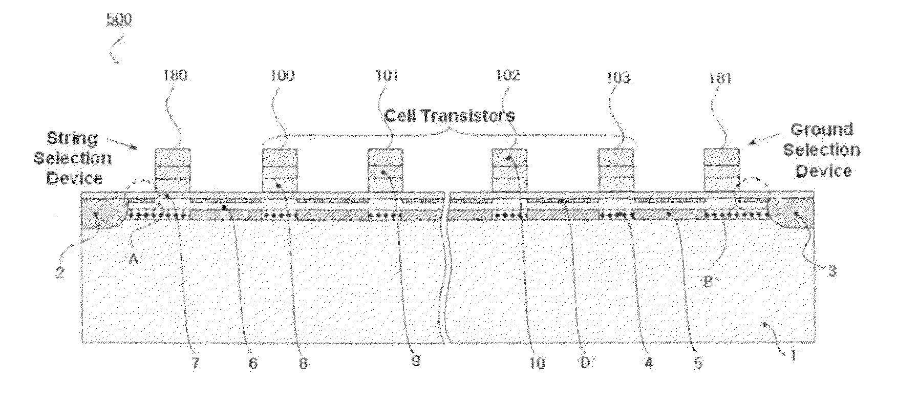
[0036]Hereinafter, the structure and operation of a high-integration NAND flash memory cell string according to embodiments of the present invention will be described in detail with reference to the attached drawings. From the drawings, insulating layers, contacts, metal wires, etc. are excluded in order to clearly show the principal characteristics of the present invention.

[0037]FIGS. 1A and 1B are sectional views of a NAND flash memory cell string according to embodiments of the present invention. Referring to FIG. 1A, a flash memory cell string 500 according to an embodiment of the present invention includes a plurality of cell devices (cell transistors) 100, 101, 102 and 103, a first switching device 180, and a second switching device 181. Referring to FIG. 1B, a flash memory cell string 501 according to another embodiment of the present invention includes a plurality of cell devices 100, 101, 102 and 103, a first switching device 182 and a second switching device 183. The diffe...


PUM


Abstract

The present invention relates to a flash memory cell string. The flash memory cell string includes a plurality of cell devices and switching devices connected to ends of the cell devices. Each of the cell devices includes a semiconductor substrate, and a transmissive insulating layer, a charge storage node, a control insulating layer and a control electrode sequentially formed on the semiconductor substrate. In the flash memory cell string, a buried insulating layer is provided on the semiconductor substrate between the cell device and an adjacent cell device, thus enabling an inversion layer, which performs the functions of source / drain, to be easily formed.According to the present invention, the reduction characteristics and performance of the cell devices of NAND flash memory are improved, and the inversion layer of a channel is induced through fringing electric fields from the control electrode and the charge storage node if necessary.

Description

CROSS-REFERENCE TO RELATED PATENT APPLICATION[0001]This application claims the benefit of Korean Patent Application No. 10-2007-0126674, filed on Dec. 7, 2007, in the Korean Intellectual Property Office, the disclosure of which is incorporated herein in its entirety by reference.BACKGROUND OF THE INVENTION[0002]1. Field of the Invention[0003]The present invention relates, in general, to a NAND flash memory cell string, and, more particularly, to a new NAND flash memory cell string, which improves the size reduction characteristics and performance of a MOS-based flash memory device and increase memory capacity.[0004]2. Description of the Related Art[0005]Recently, a demand for flash memory in electric home appliances and portable electronic devices has rapidly increased, and an increase in the capacity of flash memory has been continuously required. In the future, reduction in the size of a cell device to that of 20 nm is predicted.[0006]The degree of integration of NAND flash memory...

Claims


Application Information

Patent Timeline
Patent Type & Authority Patents(United States)
IPC IPC(8): H01L29/788H10B69/00
CPCH01L21/84H01L27/115H01L27/11521H01L27/11524H01L29/792H01L27/1203H01L29/42332H01L29/42348H01L29/7881H01L27/11568G11C16/0483H10B41/35H10B43/30H10B69/00H10B41/30H10B63/30
Inventor LEE, JONG-HO
Owner SEOUL NAT UNIV R&DB FOUND
Features
  • R&D
  • Intellectual Property
  • Life Sciences
  • Materials
  • Tech Scout
  • Unparalleled Data Quality
  • Higher Quality Content
  • 60% Fewer Hallucinations
Learn More