Semiconductor device and manufacturing method thereof

a technology of semiconductor devices and manufacturing methods, applied in the direction of semiconductor devices, electrical devices, transistors, etc., can solve the problems of reducing yield, deteriorating operating characteristics of thin film transistors, and reducing reliability, so as to reduce adverse effects of silicon device characteristics of the end portion of the silicon layer including the channel formation region, the effect of improving reliability

Inactive Publication Date: 2011-06-28
SEMICON ENERGY LAB CO LTD
View PDF46 Cites 11 Cited by
  • Summary
  • Abstract
  • Description
  • Claims
  • Application Information

AI Technical Summary

Benefits of technology

[0014]Because of such a problem due to the end portion of the island-shaped silicon layer, operating characteristics of a thin film transistor are deteriorated and the reliability is also reduced. Further, the yield is decreased in manufacturing a semiconductor device, which leads to increase of manufacturing cost. The present invention is made in view of the foregoing problems, and it is an object of the present invention to provide a semiconductor device having a novel structure in which the reliability is increased and a manufacturing method thereof.
[0017]According to another structure of the semiconductor device of the present invention, an SOI substrate in which an insulating layer and an island-shaped silicon layer are stacked in order over a support substrate, a gate insulating layer provided over one surface and a side surface of the island-shaped silicon layer, and a gate electrode which is provided over the island-shaped silicon layer with the gate insulating layer interposed therebetween and which is provided so as to get across the island-shaped silicon layer are included, and as for the gate insulating layer, the thickness in the region which is in contact with the side surface of the island-shaped silicon layer is larger and the dielectric constant in the same region is lower than those over the one surface of the island-shaped silicon layer.
[0033]By employing the present invention, defects due to an end portion of a silicon layer including a channel formation region can be reduced. Therefore, an adverse effect on a semiconductor device due to characteristics of the end portion of the silicon layer can be reduced, whereby a semiconductor device in which the reliability is improved can be provided. Further, in manufacturing a semiconductor device, the yield can be improved.

Problems solved by technology

Because of such a problem due to the end portion of the island-shaped silicon layer, operating characteristics of a thin film transistor are deteriorated and the reliability is also reduced.
Further, the yield is decreased in manufacturing a semiconductor device, which leads to increase of manufacturing cost.

Method used


Image

  • Semiconductor device and manufacturing method thereof
  • Semiconductor device and manufacturing method thereof
  • Semiconductor device and manufacturing method thereof

Examples


embodiment mode 1

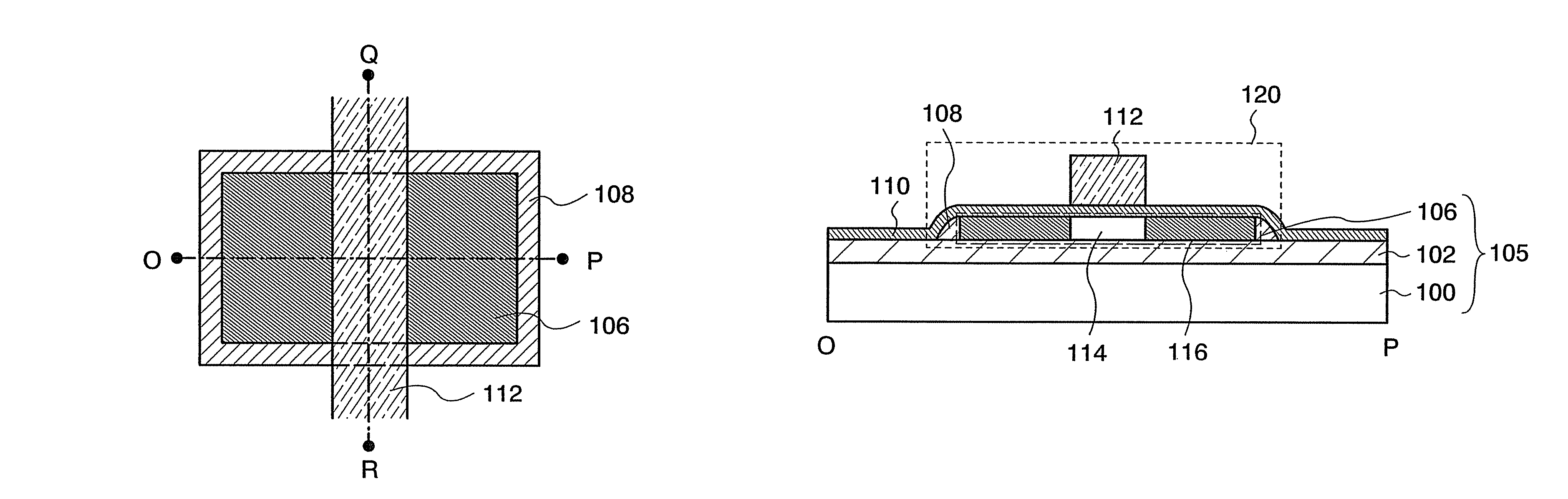
[0066]FIG. 1A is a top diagram and FIGS. 1B and 1C are cross-sectional diagrams for describing a main structure of a semiconductor device of the present invention. FIGS. 1A to 1C particularly show a structure of a thin film transistor; FIG. 1A is a top diagram, FIG. 1B is a cross-sectional diagram along a dashed line O-P in FIG. 1A, and FIG. 1C is a cross-sectional diagram along a dashed line Q-R in FIG. 1A. Note that a thin film and the like are partially omitted in FIG. 1A.

[0067]A thin film transistor 120 shown in FIG. 1A is formed using an SOI substrate 105. The thin film transistor 120 includes a silicon layer 106 in the SOI substrate 105, an insulating layer 108 which is provided so as to be in contact with a side surface of the silicon layer 106, an insulating layer 110 which is provided over one surface of the silicon layer 106, and a conductive layer 112 which is provided over the silicon layer 106 with the insulating layer 110 interposed therebetween.

[0068]As the SOI substr...

embodiment mode 2

[0119]In this embodiment mode, an example of manufacturing a semiconductor device by a manufacturing method which is different from that in Embodiment Mode 1 is described with reference to FIGS. 4A, 4B-1 and 4B-2, 4C-1 and 4C-2, 5A-1 and 5A-2, 5B-1 and 5B-2, 5C-1 and 5C-2, and 6A to 6F.

[0120]FIG. 4A is a top diagram for describing a main structure of a semiconductor device of the present invention. Note that a thin film and the like are partially omitted in FIG. 4A.

[0121]In a semiconductor device shown in FIG. 4A, a thin film transistor is formed using an SOI substrate. A surface silicon layer of the SOI substrate is formed into an island shape, and a conductive layer 314 which forms a gate electrode is provided so as to get across the island-shaped silicon layer 313. Further, an insulating layer 310 is provided so as to be in contact with the side surface of the island-shaped silicon layer 313. Although the example in which the insulating layer 310 is provided around the island-sha...

embodiment mode 3

[0159]In this embodiment mode, an example of manufacturing a semiconductor device by a manufacturing method which is different from those in the above embodiment modes is described with reference to FIGS. 7A, 7B-1 and 7B-2, 7C-1 and 7C-2, 8A-1 and 8A-2, 8B-1 and 8B-2, 8C-1 and 8C-2, and 9A to 9F.

[0160]FIG. 7A is a top diagram for describing a main structure of a semiconductor device of the present invention. Note that a thin film and the like are partially omitted in FIG. 7A.

[0161]In a semiconductor device shown in FIG. 7A, a thin film transistor is formed using an SOI substrate. A surface silicon layer 414 of the SOI substrate is formed into an island shape, and a conductive layer 417 and a conductive layer 418 which form a gate electrode are provided so as to get across the island-shaped silicon layer 414. Further, an insulating layer 410 is provided so as to be in contact with the side surface of the island-shaped silicon layer 414. Although the example in which the insulating la...


PUM


Abstract

A semiconductor device manufactured utilizing an SOI substrate, in which defects due to an end portion of an island-shaped silicon layer are prevented and the reliability is improved, and a manufacturing method thereof. The following are included: an SOI substrate in which an insulating layer and an island-shaped silicon layer are stacked in order over a support substrate; a gate insulating layer provided over one surface and a side surface of the island-shaped silicon layer; and a gate electrode which is provided over the island-shaped silicon layer with the gate insulating layer interposed therebetween. The gate insulating layer is formed such that the dielectric constant in the region which is in contact with the side surface of the island-shaped silicon layer is lower than that over the one surface of the island-shaped silicon layer.

Description

BACKGROUND OF THE INVENTION[0001]1. Field of the Invention[0002]The present invention relates to a semiconductor device manufactured using an SOI (Silicon On Insulator) substrate and a manufacturing method thereof.[0003]2. Description of the Related Art[0004]In recent years, VLSI technology has been drastically progressed, and an SOI structure by which speeding up and low power consumption are realized has been attracted attention. In this technology, an active region (a channel formation region) of a field effect transistor (FET), which has been conventionally formed of a bulk single crystal silicon, is formed of a thin-film single crystal silicon.[0005]In a substrate used for the SOI structure, a thin-film silicon layer is formed over a single crystal silicon substrate with a buried oxide film layer interposed therebetween. Therefore, it has been known that when a MOS (Metal Oxide Semiconductor) field effect transistor (MOSFET) is manufactured using an SOI substrate, the parasitic...

Claims


Application Information

Patent Timeline
Patent Type & Authority Patents(United States)
IPC IPC(8): H01L29/10H01L29/76H01L31/112H01L31/036
CPCH01L21/84H01L27/1203H01L29/78609H01L29/66772H01L29/4908H01L29/42364H01L29/51
Inventor YAMAZAKI, SHUNPEIIKEDA, KAZUKOSASAGAWA, SHINYASUZAWA, HIDEOMI
Owner SEMICON ENERGY LAB CO LTD
Why Eureka
Try Eureka