Patterning 3D features in a substrate

a technology of 3d features and substrates, applied in the field of patterning 3d features in substrates, can solve the problem of non-conventional thin-film techniques, and achieve the effect of reducing the amount of chang

Inactive Publication Date: 2011-07-26
APPLIED MATERIALS INC
View PDF6 Cites 6 Cited by
  • Summary
  • Abstract
  • Description
  • Claims
  • Application Information

AI Technical Summary

Benefits of technology

[0009]It is highly desirable to minimize the amount of change introduced when optimizing a new process or when compensating for other minor fluctuations in the process flow. With a simple tuning of only the relative ratio of process gases, radii of curvature in silicon lenses have been demonstrated ranging from 100 μm to 1 mm, having diameters in-plane ranging from 100 μm to 500 μm.

Problems solved by technology

To form optical surfaces apart from these two planes requires non-conventional thin-film techniques.

Method used


Image

  • Patterning 3D features in a substrate
  • Patterning 3D features in a substrate
  • Patterning 3D features in a substrate

Examples


Embodiment Construction

Fabricating a Lens

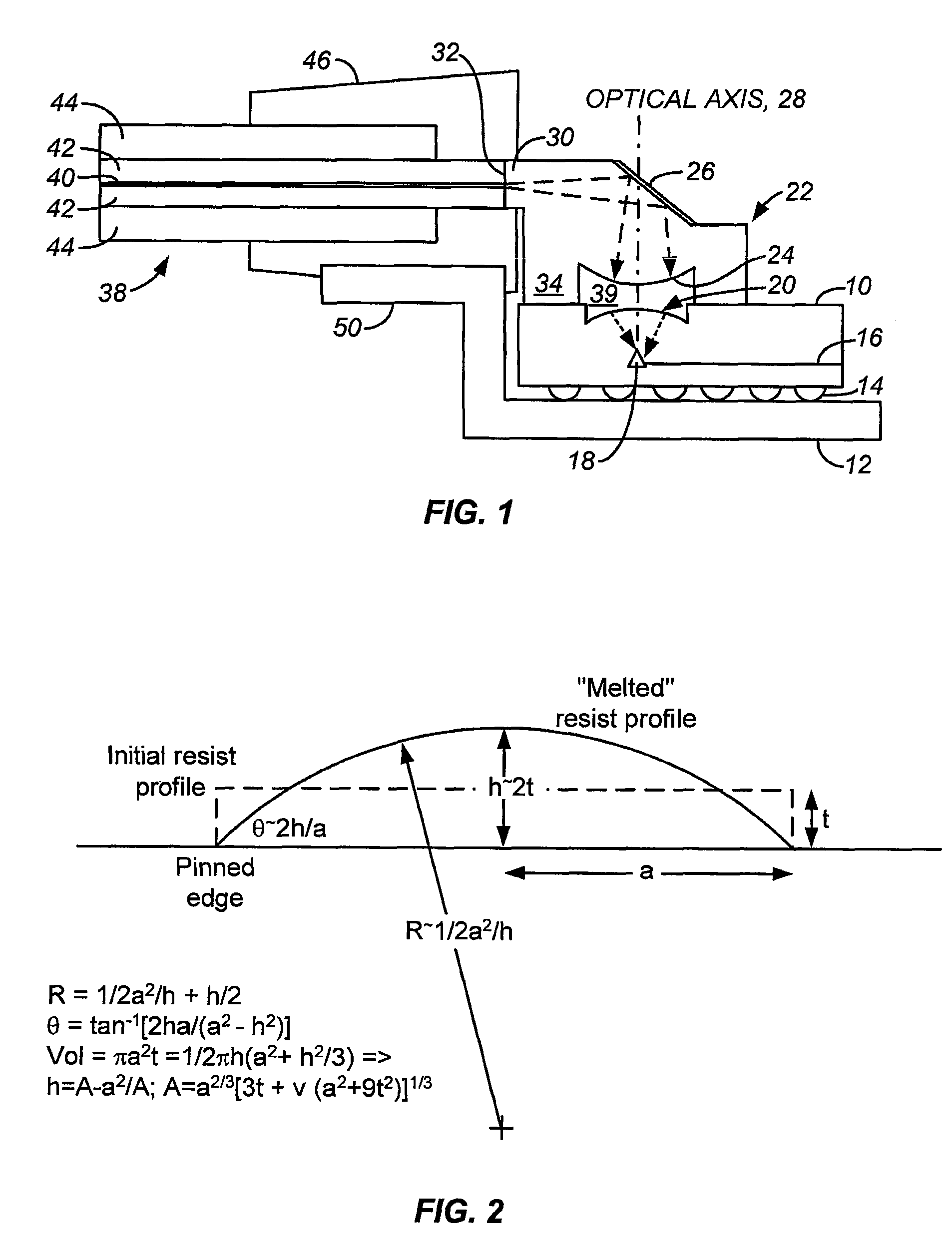
[0033]FIG. 1 shows a circuit assembly which includes a silicon IC chip 10 with a lens 20 formed on its back surface in order to provide a way to couple optical signals into and out of the optical circuitry that is fabricated on the chip. IC chip 10 is flip-chip mounted onto a chip carrier 12 by means of a ball grid array (BGA) 14. Using known techniques, such as those described in U.S. Ser. No. 10 / 280,492 entitled “Optical Ready Wafers,” an optical waveguide 16 has been fabricated on the front side of the chip. Waveguide 16 is either fabricated in a layer within the chip that is at the same level as other microelectronic (e.g. CMOS) circuitry (not shown) that is also fabricated on the front side of the chip or it is in a layer that is buried beneath the level in which the microelectronic circuitry resides. Optical waveguide 16 represents an optical signal distribution network that serves to distribute optical clock signals or other optical signals to and / or from th...


PUM

PropertyMeasurementUnit
angleaaaaaaaaaa
widthaaaaaaaaaa
widthaaaaaaaaaa

Abstract

Methods of forming a 3D structure in a substrate are disclosed. A layer of resist is deposited on the substrate. The layer of resist is patterned to define an edge at a predetermined location. The resist is reflowed to form a tapered region extending from the etch. Both the reflowed resist and the substrate are concurrently etched to transfer the tapered profile of the reflowed resist into the underlying substrate to form an angled surface. The etching is discontinued before all of the resist is consumed by the etching.

Description

CROSS-REFERENCES TO RELATED APPLICATIONS[0001]This application is a nonprovisional of, and claims the benefit of the filing date of, U.S. Prov. Pat. Appl. No. 60 / 805,010, entitled “Patterning 3D Features in a Substrate,” filed Jun. 16, 2006 by Eric Perozziello et al, the entire disclosure of which is incorporated herein by reference for all purposes.BACKGROUND OF THE INVENTION[0002]Optical components are now being integrated in chips along side microelectronic components. An example of one such approach is described in U.S. Ser. No. 10 / 280,505, entitled “Optical Ready Substrates,” incorporated herein by reference. Basically, it is a semiconductor wafer into which optical signal distribution network made up of optical waveguides, optical detectors, and other optical components has been fabricated in anticipation of the subsequent fabrication of microelectronic circuitry above the optical network. The optical sign distribution network is designed to carry optical signals (e.g. clock o...

Claims


Application Information

Patent Timeline
Patent Type & Authority Patents(United States)
IPC IPC(8): H01L21/302H01L21/461
CPCG02B6/12002G02B6/136H01L21/0334H01L21/3083G02B6/4214
Inventor PEROZZIELLO, ERICKROPEWNICKI, THOMAS JOSEPHWOJCIK, GREGORY L.GOEBEL, ANDREASBJORKMAN, CLAES
Owner APPLIED MATERIALS INC
Why Eureka
Try Eureka