
Distributing power to an integrated circuit

a technology of integrated circuits and power supplies, applied in emergency protective arrangements for limiting excess voltage/current, emergency protective arrangements for automatic disconnection, dc source parallel operation, etc., can solve problems such as failure to work and surge current degradation, and achieve the effect of increasing the space required for input/output cells to be attached to the integrated circuit and increasing the width of the portion

Active Publication Date: 2011-07-26
ARM LTD
View PDF4 Cites 0 Cited by
  • Summary
  • Abstract
  • Description
  • Claims
  • Application Information

AI Technical Summary

Benefits of technology

The present invention provides a power supply cell for distributing power to an integrated circuit. The cell has two conductive paths for current flow: a first path and a second path. The first path has a lower resistance than the second path, allowing for increased power distribution. The cell also has a layer of conductive material that is arranged to provide a path for surge current flow and protect the circuit from electrostatic discharge. The conductive material is arranged to have a significantly lower resistance in the first path than in the second path, with the second path having a higher resistance. The cell can be widened to provide additional power without increasing the size of the integrated circuit. The width of the cell can be greater than the pitch width of the integrated circuit. The technical effect of the invention is to provide a more efficient and effective power supply cell for integrated circuits.

Problems solved by technology

However, there is a limit as these conduction paths need to carry the surge current that is produced by an electrostatic discharge.
Clearly, if they have too high a resistance then they will degrade under the surge current and will not work.

Method used


Image

  • Distributing power to an integrated circuit
  • Distributing power to an integrated circuit
  • Distributing power to an integrated circuit

Examples


Embodiment Construction

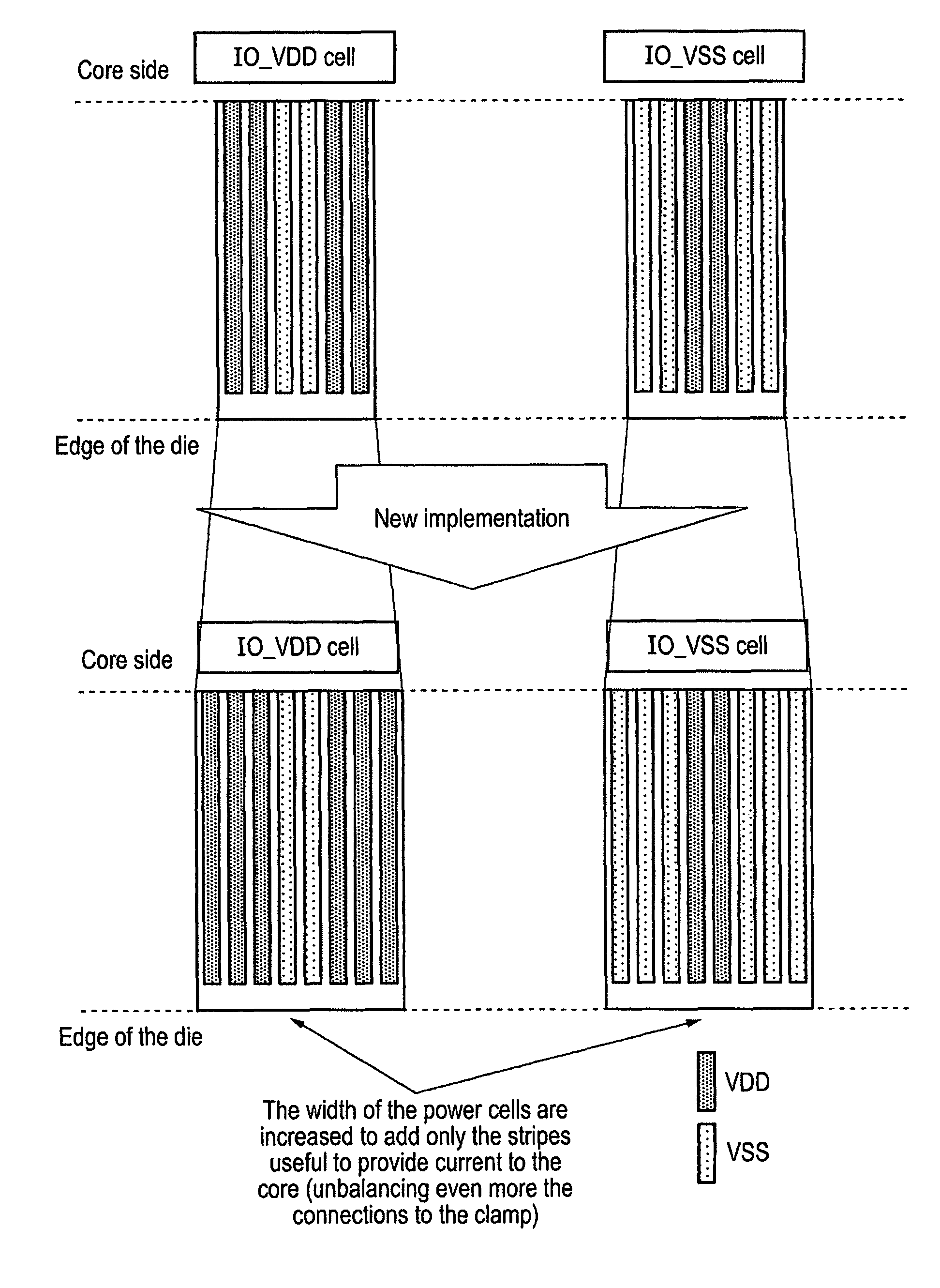
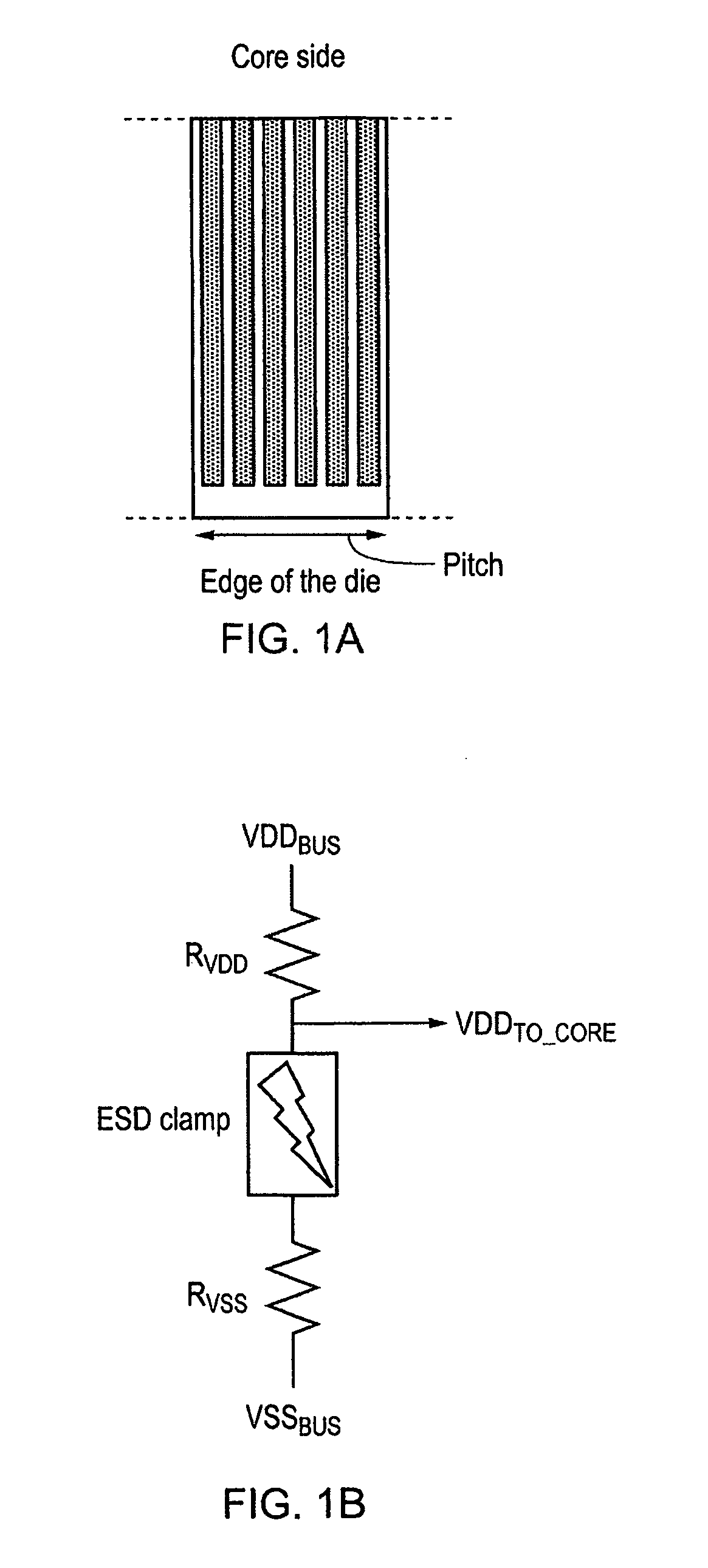
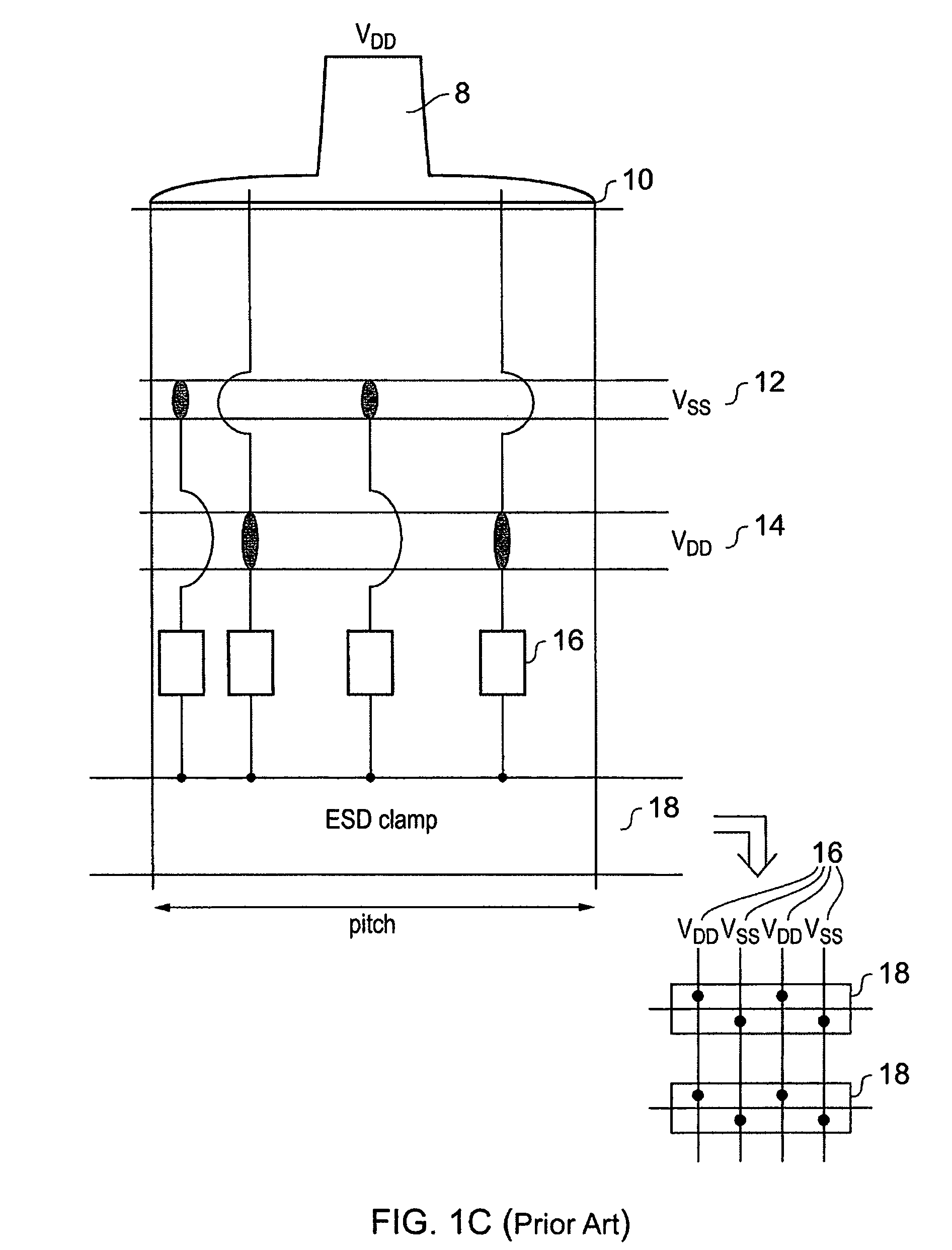
[0043]FIG. 2 shows an integrated circuit 30 that comprises a core 40 and an input / output loop 50 that comprises power cells 52 and 54 and the input / output cell 56. Power cell 52 is connected to a low voltage power supply VSS, while power cell 54 is connected to a high level voltage supply VDD. Each of these cells are a width w wide which is the pitch of the device and is the minimum width for providing bonding of a wire. In many integrated circuits nowadays this is the determining factor in size and for this reason the core 40 lies well within this input / output loop.

[0044]The power cells 52 and 54 have several layers and FIG. 3 shows one of these cells schematically in cross section. There is a top layer which is the bonding layer 60 to which the wires are bonded. There is then the layer that the power rails lie in. These are rails 12 and 14 that carry VSS and VDD around the loop of the cell. The next layer down is the layer providing the metallisation contacts that take the power f...


PUM


Abstract

A power supply cell for distributing power supplied from a first voltage supply to an integrated circuit is disclosed. The power supply cell comprises: a layer comprising conductive material, the conductive material providing a conduction path for current flowing from the first voltage supply to a portion of the integrated circuit to be powered and further providing a protection path for surge current flowing between the first voltage supply and an electrostatic discharge protection device and between the electrostatic discharge protection device and the second voltage supply; the conductive material forming a first conduction path for providing a path for current flowing between the first voltage supply and the portion of the integrated circuit to be powered and for providing a portion of the protection path for surge current flowing between the first voltage supply and the electrostatic discharge protection device and a second conduction path for providing a further portion of the protection path for surge current flowing between the second voltage supply and the electrostatic discharge protection device; wherein the conductive material is arranged such that the first conduction path has a significantly lower resistance than the second conduction path.

Description

BACKGROUND OF THE INVENTION[0001]1. Field of the Invention[0002]The field of the invention relates to integrated circuits and in particular to supplying power to the integrated circuits.[0003]2. Description of the Prior Art[0004]With advances in semiconductor technology, semiconductor chips are getting ever smaller and a limiting factor to the decrease in the size of the device is now often the size of the area required to bond a wire to the device so that external signals and power can be supplied to the device. Such chips are termed pad limited and over 90% of chips now fall within this category.[0005]The minimum width of the area required to bond a wire to a device is termed the pitch of the device. When supplying power to a semiconductor core a power pad is used to provide a connection between the wire bonded to the device and the core. Cores need to be protected from electrostatic discharge which can cause surge currents and local heating of the device, and this is done using E...

Claims


Application Information

Patent Timeline
Patent Type & Authority Patents(United States)
IPC IPC(8): H02H9/00
CPCH02J1/00
Inventor RIEN, MIKAELBLANC, FABRICEKUMAR, NIDHIR
Owner ARM LTD
Learn More