Lateral power MOSFET with high breakdown voltage and low on-resistance

a technology of lateral power mosfet and low breakdown voltage, which is applied in the direction of semiconductor devices, semiconductor/solid-state device details, electrical apparatus, etc., can solve the problems of less efficient devices, low breakdown voltage, and inability to maintain a low on-resistance, so as to improve the performance and efficiency of semiconductor devices, reduce the on-resistance of devices, and increase the breakdown voltage of devices

Inactive Publication Date: 2011-08-02
TAIWAN SEMICON MFG CO LTD
View PDF20 Cites 7 Cited by
  • Summary
  • Abstract
  • Description
  • Claims
  • Application Information

AI Technical Summary

Benefits of technology

[0015]By using these configurations in semiconductor devices and lateral power MOSFETs that have an extended drift region, the on-resistance of the device is reduced and the breakdown voltage of the device is increased. These all work to improve the performance and efficiency of the semiconductor device.

Problems solved by technology

A problem with this type of lateral power MOSFET is that it cannot maintain a low on-resistance when a high voltage is passed through the lateral power MOSFET.
The larger the on-resistance of the device, the less efficient the device.
Another problem with the prior art device 100 (shown in FIG. 1A) and the prior art device 150 (shown in FIG. 1B) is that the breakdown voltage is not as high as desired.
When a voltage greater than the breakdown voltage is applied, catastrophic and irreversible damage is done to the device, rendering the devices commercially useless and requiring the device to be replaced.
Those prior art systems, however, have difficulties sustaining high voltage and low on-resistance.

Method used


Image

  • Lateral power MOSFET with high breakdown voltage and low on-resistance
  • Lateral power MOSFET with high breakdown voltage and low on-resistance
  • Lateral power MOSFET with high breakdown voltage and low on-resistance

Examples


Embodiment Construction

[0029]The making and using of the presently preferred embodiments are discussed in detail below. It should be appreciated, however, that the present invention provides many applicable inventive concepts that can be embodied in a wide variety of specific contexts. The specific embodiments discussed are merely illustrative of specific ways to make and use the invention, and do not limit the scope of the invention.

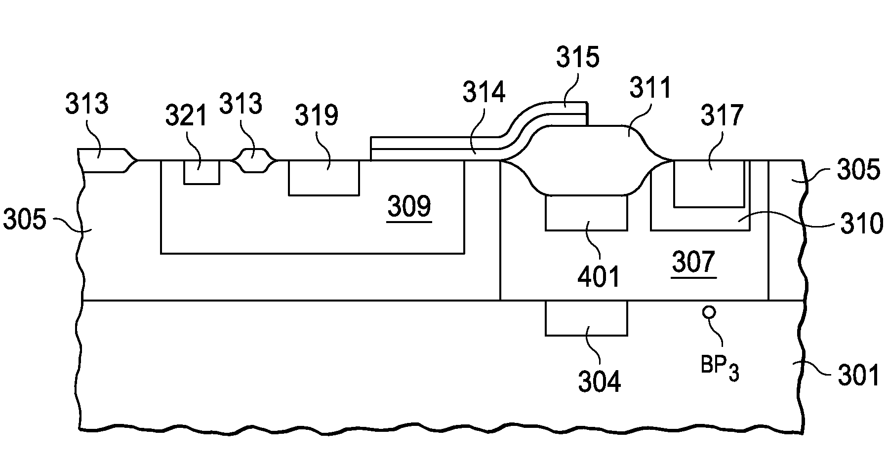
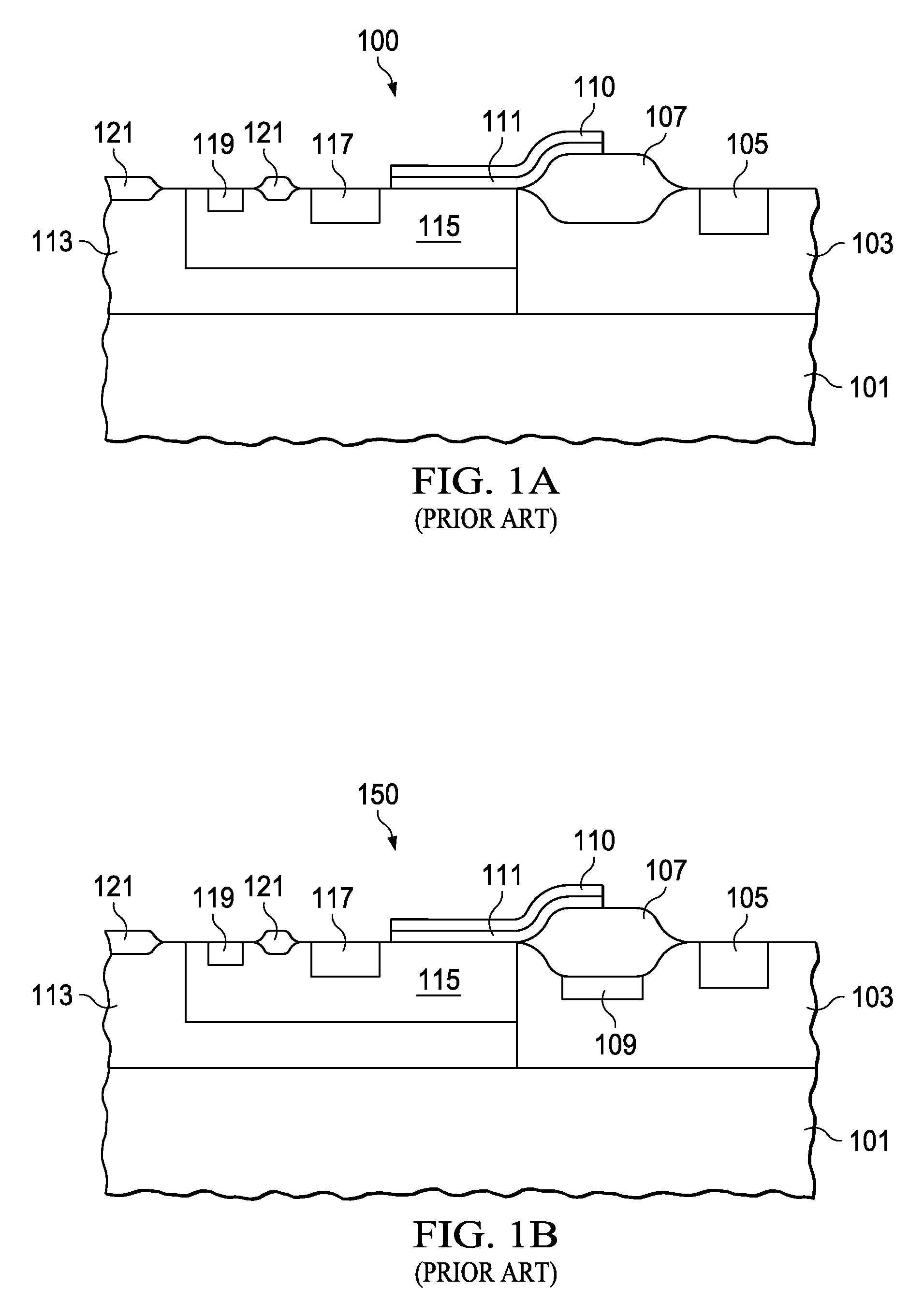
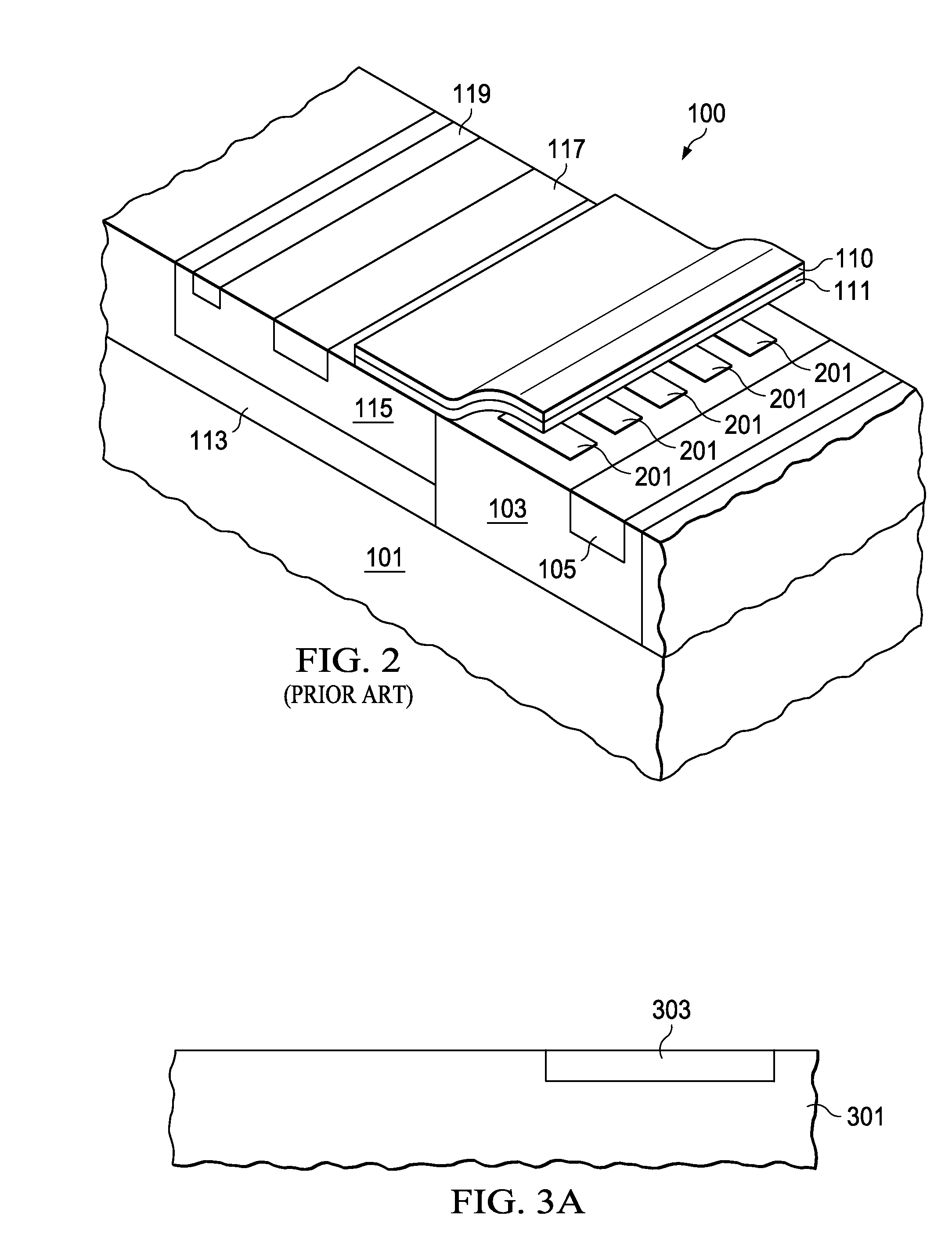
[0030]A novel (ultra) high-voltage metal-oxide-semiconductor field-effect transistor (MOSFET) having a reduced on-resistance, an increased breakdown voltage, and an increased stability, and the methods of forming the same are provided. Embodiments of the present invention may be useful for lateral power MOSFETs, particularly when the device is under a high voltage. Throughout the description, the terms “ultra high-voltage MOSFET” and “lateral power MOSFET” are equally referred to. The manufacturing processes are detailed in the following paragraphs. Throughout the various vie...


PUM


Abstract

A semiconductor structure includes a semiconductor substrate of a first conductivity type; a pre-high-voltage well (pre-HVW) in the semiconductor substrate, wherein the pre-HVW is of a second conductivity type opposite the first conductivity type; a high-voltage well (HVW) over the pre-HVW, wherein the HVW is of the second conductivity type; a field ring in the HVW and occupying a top portion of the HVW, wherein the field ring is of the first conductivity type; an insulation region over and in contact with the field ring and a portion of the HVW; a gate electrode partially over the insulation region; a drain region in the HVW, wherein the drain region is of the second conductivity type; and wherein the HVW horizontally extends further toward the drain region than the pre-HVW; and a source region adjacent to, and on an opposite side of the gate electrode than the drain region.

Description

[0001]The present application is a continuation-in-part of U.S. patent application Ser. No. 11 / 581,178, filed Oct. 13, 2006 now U.S. Pat. No. 7,476,591, and entitled “Lateral Power MOSFET with High Breakdown Voltage and Low On-Resistance,” which patent application is hereby incorporated herein by reference.TECHNICAL FIELD[0002]This invention relates generally to semiconductor structures and methods, and more particularly to a lateral power metal oxide semiconductor field effect transistor (MOSFET).BACKGROUND[0003]A lateral power MOSFET is basically a metal oxide semiconductor field effect transistor fabricated with coplanar drain and source regions. FIG. 1A shows a lateral power MOSFET device 100 in the prior art. The device 100 is formed on a p-type substrate 101 and another p-layer 113 is epitaxially grown on the substrate 101. A high-voltage P-well 115 is adjacent a high-voltage N-well 103 in the epitaxially grown p-layer 113. An N+ source 117 is positioned in the high-voltage P-...

Claims


Application Information

Patent Timeline
Patent Type & Authority Patents(United States)
IPC IPC(8): H01L29/78
CPCH01L29/063H01L29/0634H01L29/0847H01L29/66659H01L29/7835H01L29/0692H01L29/42368
Inventor HUANG, TSUNG-YICHIANG, PUO-YULIU, RUEY-HSINHSU, SHUN-LIANGHUANG, CHYI-CHYUANCHEN, FU-HSINHUANG, ERIC
Owner TAIWAN SEMICON MFG CO LTD
Why Eureka
Try Eureka