

Wafer level integration module with interconnects
a technology of interconnection and integrated circuit, which is applied in the direction of electrical testing, instruments, electrical apparatus, etc., can solve the problems of cumbersome handling of wafers, time-consuming and time-consuming cutting notches, and limited i/o density of ic devices that are fabricated by conventional processes
- Summary
- Abstract
- Description
- Claims
- Application Information
AI Technical Summary
Benefits of technology
Problems solved by technology
Method used
Image

Examples
Embodiment Construction
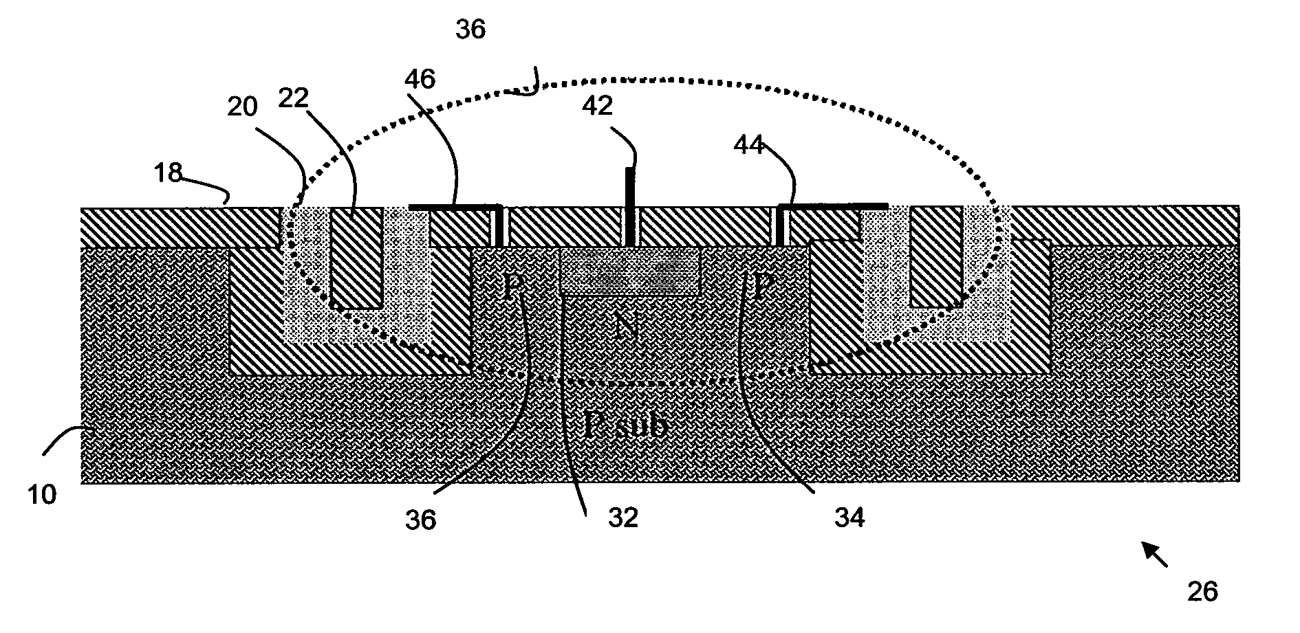
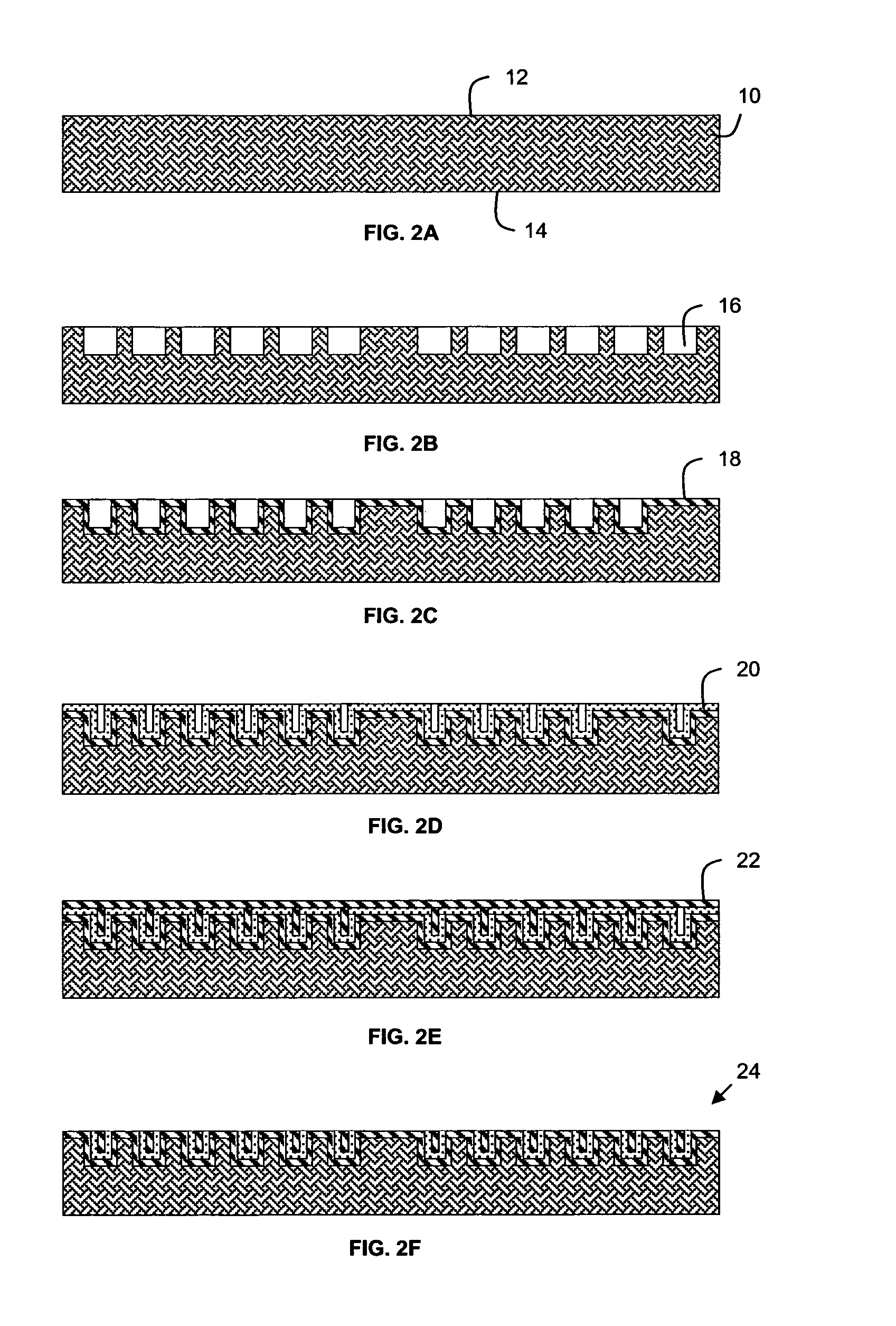
[0021]According to an embodiment of the present invention, there is provided a method 200 of manufacturing an integrated circuit (IC) device 90. According to the method, a wafer 10 is first provided having a first or top surface and a second or bottom surface. The wafer may be a blank polished or unpolished silicon wafer or the like. High aspect ratio micro-structures 16 that are specifically designed to provide a die level interconnect configuration and mapping, are provided on the first blank surface 12 of the wafer. The wafer with pre-formed conductive interconnect microstructures 16 are further processed for device fabrication, for example, at the wafer fabrication facilities. Once the front side 12 devices are fabricated, the silicon material 20 is then removed from a second side 14 of the device wafer 10, opposite the first side, to expose the high temperature conductive interconnect microstructures 16. Contacts are formed on the second side of the device wafer using conductiv...
PUM
 Abstract
Description
Claims
Application Information