Discrete wafer array process

a technology of discrete wafers and arrays, which is applied in the direction of basic electric elements, electrical equipment, and semiconductor devices, etc., can solve the problems of unreliability of commercially available silicon pressure sensors, inability to manufacture large-scale, and increased upper temperature limits, so as to achieve greater ruggedness, higher temperature conductivity, and high temperature resistance

Inactive Publication Date: 2001-06-19
OKOJIE ROBERT S
View PDF2 Cites 28 Cited by
  • Summary
  • Abstract
  • Description
  • Claims
  • Application Information

AI Technical Summary

Benefits of technology

It is an object of this invention to disclose a method of fabricating SiC wafers in an array on an amorphous substrate. The substrate need not be crystalline. It may be selected to have higher temperature resistance, higher temperature conductivity, and greater ruggedness than silicon. SiC has a higher coefficient of thermal expansion than silicon. In extreme temperature variations this is critical. High thermal conductivity also allows the substrate to act as a heat sink. It facilitates connection of pins thereto and may provide a radiation shield. It is particularly advantageous when integrated devices thereon comprise power transistors. Greater ruggedness is generally advantageous; the substrate may act as a circuit board. It is particularly advantageous in vibration. It is yet a further object of this invention to disclose a method which provides for the production of a precisely positioned array of wafers on a substrate. Tight process control facilitates tight packing and minimal waste. Additionally it is not necessary to undertake expensive epitaxial growth on small multiple surfaces. The cost of conventional SiC wafer production may be reduced by more than an order of magnitude. It is yet a further object of this invention to disclose a method of SiC fabrication which will facilitate production of optimally thin wafers--wafers which will have minimal parasitics when used in devices. Very thin SiC wafers also enable epitaxial growth on a top surface thereof. A final object of this invention is to disclose a structure which will facilitate integrating microelectromechanical devices with CMOS controls, and amplification circuits, on the same substrate.

Problems solved by technology

Commercially available silicon pressure sensors become unreliable above 200.degree. C.
Silicon on Insulator technology has enabled device operation to 300.degree. C., and with costly integrated cooling systems this upper temperature limit has further increased.
Large scale production is inhibited by the small size of applicable SiC wafers due to incompatability with conventional semiconductor fabrication facilities.
One problem with Malhi's structure is that its thermal budget is limited by the silicon substrate.
The mismatch in coefficient of thermal expansion between SiC and silicon has the potential to create reliability problems.
Another inherent problem with Malhi's structure is that the SiC wafers cannot be precisely and consistently positioned on the silicon substrate.
Consequently they cannot be tightly packed.
They lack much needed process control.

Method used


Image

  • Discrete wafer array process
  • Discrete wafer array process

Examples


Embodiment Construction

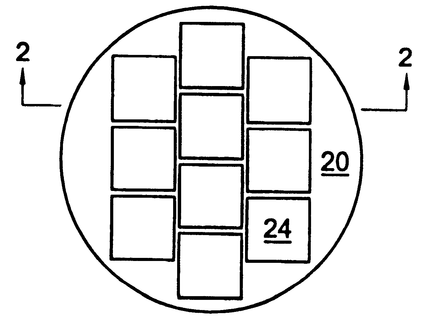
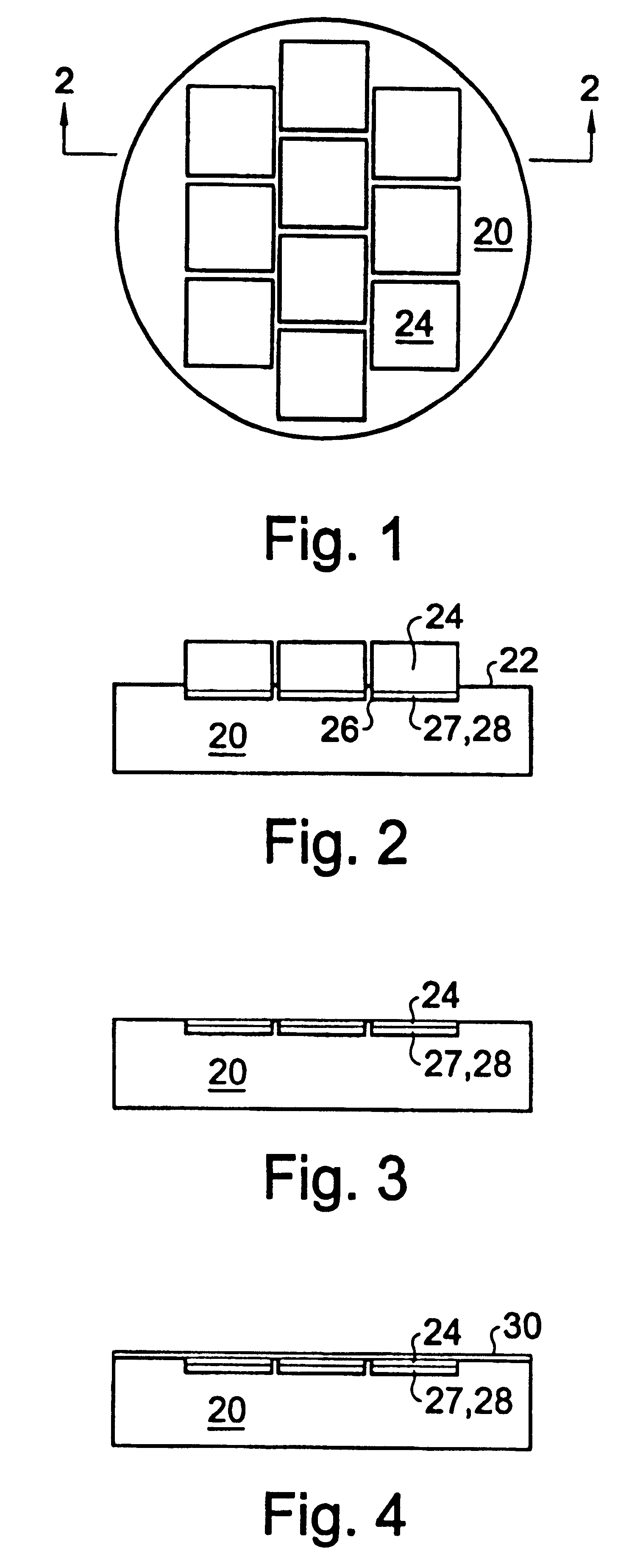
Turning now to the drawings and more particularly to FIG. 1 we have a plan view of a large wafer 20 of substrate having a face 22 indented for an array of small wafers 24 and having the small wafers 24 matingly fitted into the depressions 26 thereon. FIG. 2 is a cross sectional view of the large wafer 20 shown in FIG. 1 taken along section line 2--2 therethrough. A method of preparing small wafers 24 for compatibility with conventional large wafer fabrication equipment (not shown) comprises the following steps: indenting a face 22 of a large wafer 20 to form an array of depressions 26 thereon, each depression 26 sized to matingly accept a lower portion of a small wafer 24; applying a bonding medium 27 to an exterior side of the depressions 26 on the indented face of the large wafer 20; matingly fitting the small wafers 24 into the depressions 26 so that the small wafers 24 are positioned in an array on the large wafer 20; and, removing the top portion of the small wafers 24 standing...


PUM


Abstract

A method of preparing small wafers for compatibility with conventional large wafer fabrication equipment comprising the following steps: indenting a face of a large wafer to form an array of depressions thereon, each depression sized to matingly accept a lower portion of a small wafer; applying a bonding medium to an exterior side of the depressions on the indented face of the large wafer; matingly fitting the small wafers into the depressions so that the small wafers are positioned in an array on the large wafer; and, removing the top portion of the small wafers standing out of the depressions by chemical mechanical polishing so that the remaining portions of the small wafers then have a uniform thickness generally equal to the depth of the indentations in the large wafer. A preferred aspect of this invention provides for a method as above wherein the small wafer is SiC and the large wafer is made from an amorphous substance which comprises SiC or aluminum nitride.

Description

This invention relates to production of silicon carbide (SiC) wafers. More particularly this invention discloses a method which enables an array of small SiC wafers to be concurrently produced on a larger, industry standard sized wafer. This allows the use of industry standard equipment and dramatically increases production rates.The increasingly pervasive presence of microprocessors in controls has created an increasing demand for sensors in all types of environments so that processes may be more closely monitored, operations may be more finely tuned, and so that efficiencies and emissions may be improved.Commercially available silicon pressure sensors become unreliable above 200.degree. C. Silicon on Insulator technology has enabled device operation to 300.degree. C., and with costly integrated cooling systems this upper temperature limit has further increased. Large scale production is inhibited by the small size of applicable SiC wafers due to incompatability with conventional s...

Claims


Application Information

Patent Timeline
Patent Type & Authority Patents(United States)
IPC IPC(8): H01L21/02H01L21/67H01L21/20H01L21/306H01L21/68
CPCH01L21/30625H01L21/6835H01L2924/3025H01L2221/68313H01L21/02002
Inventor OKOJIE, ROBERT S.
Owner OKOJIE ROBERT S
Why Eureka
Try Eureka