Semiconductor device and manufacturing method thereof

a semiconductor and semiconductor technology, applied in semiconductor devices, diodes, electrical devices, etc., can solve the problems of inability to apply the above-mentioned method, the inability to recover properties, and the inability to achieve the effect of recovery property

Active Publication Date: 2011-08-16
DENSO CORP
View PDF17 Cites 7 Cited by
  • Summary
  • Abstract
  • Description
  • Claims
  • Application Information

AI Technical Summary

Benefits of technology

[0019]In a semiconductor device including a MOS transistor cell or an IGBT cell and a diode cell over a same semiconductor substrate, it is an object of the present disclosure to provide the semiconductor device, in which recovery property of the diode cell can be improved without damaging the property of the MOS transistor cell or the property of the IGBT cell and the surge withstand property does not deteriorate, and a manufacturing method thereof.

Problems solved by technology

Therefore, the recovery property becomes worse.
However, in the diode cell 90d of the semiconductor device 90, which is provided with the MOS transistor cell 90t, modification for improving the performance of the diode cell 90d may impair the performance of the MOS transistor cell 90t.
Therefore, the above-mentioned method can not be applied.

Method used


Image

  • Semiconductor device and manufacturing method thereof
  • Semiconductor device and manufacturing method thereof
  • Semiconductor device and manufacturing method thereof

Examples


first embodiment

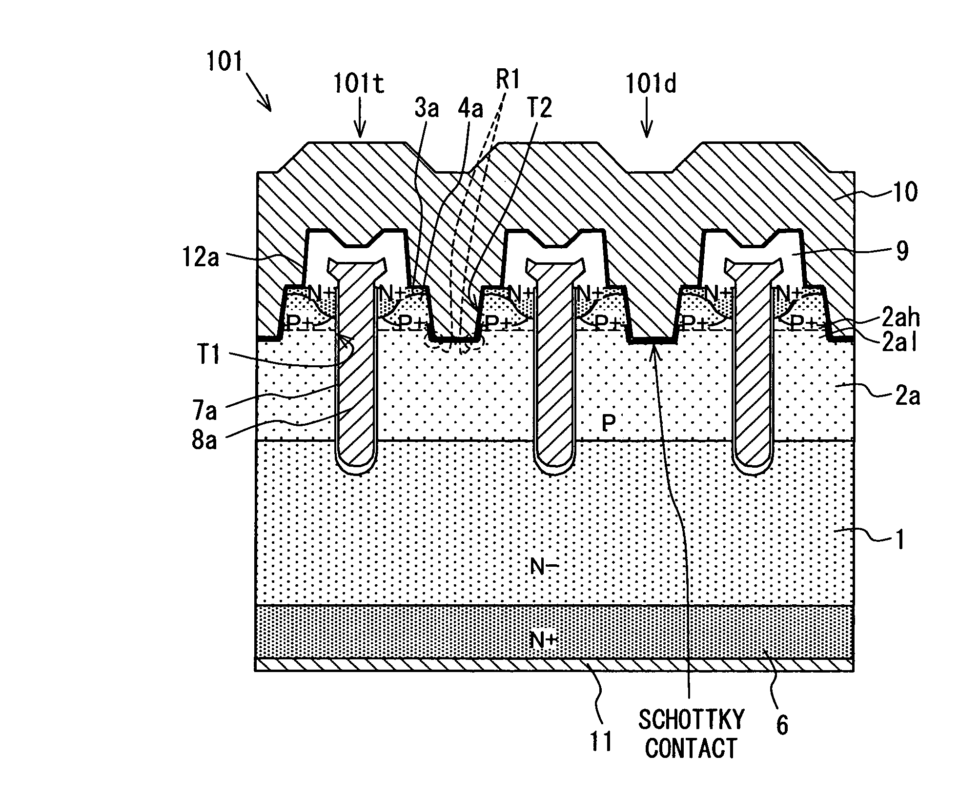
[0079]Hereinafter, a first embodiment of a semiconductor device will be described with reference to FIG. 1. FIG. 1 is a cross sectional side view (a view of a cross sectional structure seen from a side surface) of a semiconductor device 101 according to the first embodiment. As shown in FIG. 1, the semiconductor device 101 of the present embodiment has a structure based on the semiconductor device 90 shown in FIG. 15, and with respect to the same component with one included in the semiconductor device 90, the same reference numerals are applied.

[0080]As shown in FIG. 1, the semiconductor device 101 includes a semiconductor substrate 1 including both a trench type MOS transistor cell (hereinafter also referred to as “MOS transistor cell”) 101t and a diode cell 101d. In other words, a plurality of trench type MOS transistor cells 101t, each of which includes a parasitic diode cell 101d, are formed in the semiconductor substrate 1.

[0081]Specifically, in the semiconductor device 101, a ...

second embodiment

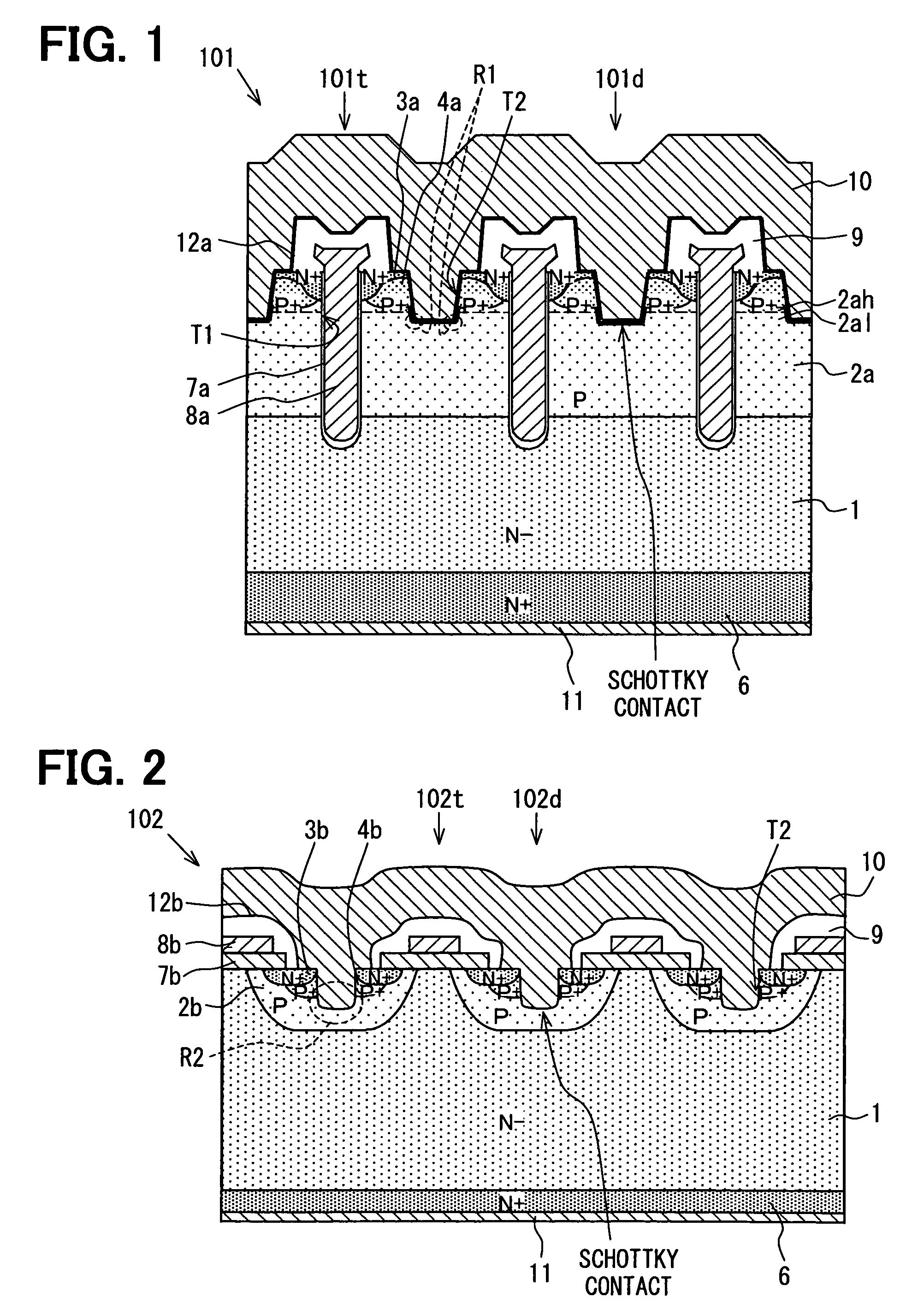
[0097]Hereinafter, a second embodiment of a semiconductor device will be described with reference to FIG. 2. FIG. 2 is a cross sectional side view of a semiconductor device according to the present embodiment.

[0098]As shown in FIG. 2, a semiconductor device 102 of the second embodiment has a structure based on the semiconductor device 101 shown in FIG. 1. That is, in the semiconductor device 102, a plurality of MOS transistor cells 102t and diode cells 102d, which are similar to the structures of the MOS transistor cell 101t and the diode cell 101d in the semiconductor device 101, are formed over the n-conductive type semiconductor substrate 1. However, the MOS transistor cell 102t is not a trench type MOS transistor in the semiconductor device 102 and a plurality of planar type MOS transistors are formed in the semiconductor substrate 1.

[0099]In other words, in the semiconductor device 102 as well as the semiconductor device 101, a p-conductive type (P) region 2b, in which an impur...

third embodiment

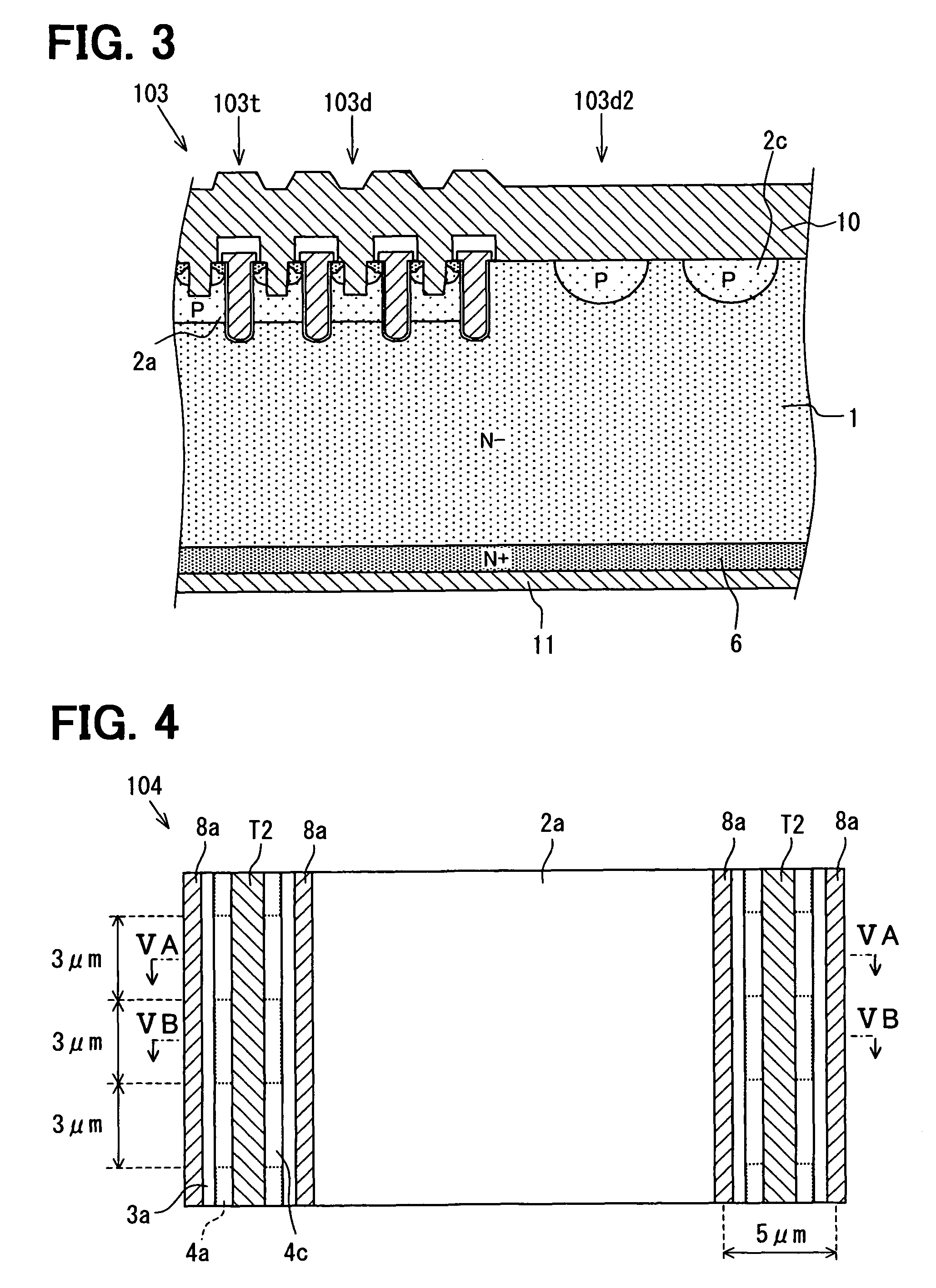
[0104]Hereinafter, a third embodiment of a semiconductor device will be described with reference to FIG. 3. FIG. 3 is a cross sectional side view of a semiconductor device according to the embodiment.

[0105]As shown in FIG. 3, a semiconductor device 103 of the present embodiment has a structure based on the semiconductor device 101 shown in FIG. 1. That is, in the semiconductor device 103, a plurality of MOS transistor cells 103t and diode cells 103d, which are similar to the structures of the MOS transistor cell 101t and the diode cell 101d in the semiconductor device 101, are formed over the n-conductive type semiconductor substrate 1.

[0106]However, as shown in FIG. 3, in the semiconductor device 103 of the present embodiment, a main side second p-conductive type (P) region 2c is arranged in the main side surface portion of the n-conductive type semiconductor substrate 1 of a region, which is a different position from the diode cell 103d, and at which the p-conductive type layer 2a...


PUM


Abstract

A semiconductor device includes an n-conductive type semiconductor substrate having a main side and a rear side, a p-conductive type layer arranged over the main side of the substrate, a main side n-conductive type region arranged in the p-conductive type layer, a rear side n-conductive type layer arranged over the rear side of the substrate, a first trench which reaches the substrate and penetrates the main side n-conductive type region and the p-conductive type layer, a second trench which reaches an inside of the p-conductive type layer, a second electrode layer, which is embedded in the second trench and connected to the p-conductive type layer. Hereby, the semiconductor device, in which the recovery property of a diode cell can be improved without damaging the property of a MOS transistor cell or an IGBT cell and the surge withstand property does not deteriorate, can be obtained.

Description

CROSS REFERENCE TO RELATED APPLICATIONS[0001]This application is based on Japanese Patent Application No. 2007-162999 filed on Jun. 20, 2007 and Japanese Patent Application No. 2008-153327 filed on Jun. 11, 2008, the disclosures of which are incorporated herein by reference.FIELD OF THE INVENTION[0002]The present invention relates to a semiconductor device having a semiconductor substrate, in which a MOS transistor cell or an IGBT cell functioning as a switching element and a diode cell functioning as a free wheel diode are arranged, and a manufacturing method thereof.BACKGROUND OF THE INVENTION[0003]An inverter circuit for driving a load such as a motor is a switching equipment between direct current and alternating current, converts the direct current to the alternating current and feeds the alternating current voltage into the motor as the load. The inverter circuit for driving an inductive motor includes a MOS transistor as a switching element and a free wheel diode. The MOS tra...

Claims


Application Information

Patent Timeline
Patent Type & Authority Patents(United States)
IPC IPC(8): H01L29/66H01L29/78H01L21/8234H01L21/336H01L29/772
CPCH01L21/26586H01L29/1095H01L29/7813H01L29/66727H01L29/66734H01L29/7397H01L29/7806H01L29/41766H01L29/0619H01L29/0696
Inventor TSUZUKI, YUKIOASAI, MAKOTO
Owner DENSO CORP
Why Eureka
Try Eureka