Semiconductor integrated circuit

a technology of integrated circuits and semiconductors, applied in logic circuit coupling/interface arrangements, pulse techniques, instruments, etc., can solve problems such as inaccurate data transmission between data transmitting circuits and data receiving circuits, and achieve the effect of reducing power supply nois

Active Publication Date: 2011-08-16
RENESAS ELECTRONICS CORP
View PDF5 Cites 25 Cited by
  • Summary
  • Abstract
  • Description
  • Claims
  • Application Information

AI Technical Summary

Benefits of technology

[0007]In the related art, the countermeasure such as an ODT function has been provided to reduce the power-supply noise which influences the data receiving circuit. However, the related art provides no countermeasure to reduce the power-supply noise which influences the data transmitting circuit. Normally, the data transmitting circuit includes a data output circuit such as a three-state buffer for transmitting data. The data transmitting circuit controls the data output circuit to output or not to output the data based on a control signal.
[0018]With the circuit structure as described above, it is possible to transmit data accurately by reducing the amplification of the power-supply noise.
[0019]According to an exemplary aspect of the present invention, it is possible to provide a semiconductor integrated circuit capable of transmitting data accurately.

Problems solved by technology

In a semiconductor integrated circuit, there has been a problem that data transmission between a data transmitting circuit and a data receiving circuit is not accurately executed when power-supply noise occurs on a plurality of signal lines used for the data transmission between these circuits.

Method used


Image

  • Semiconductor integrated circuit
  • Semiconductor integrated circuit
  • Semiconductor integrated circuit

Examples


first exemplary embodiment

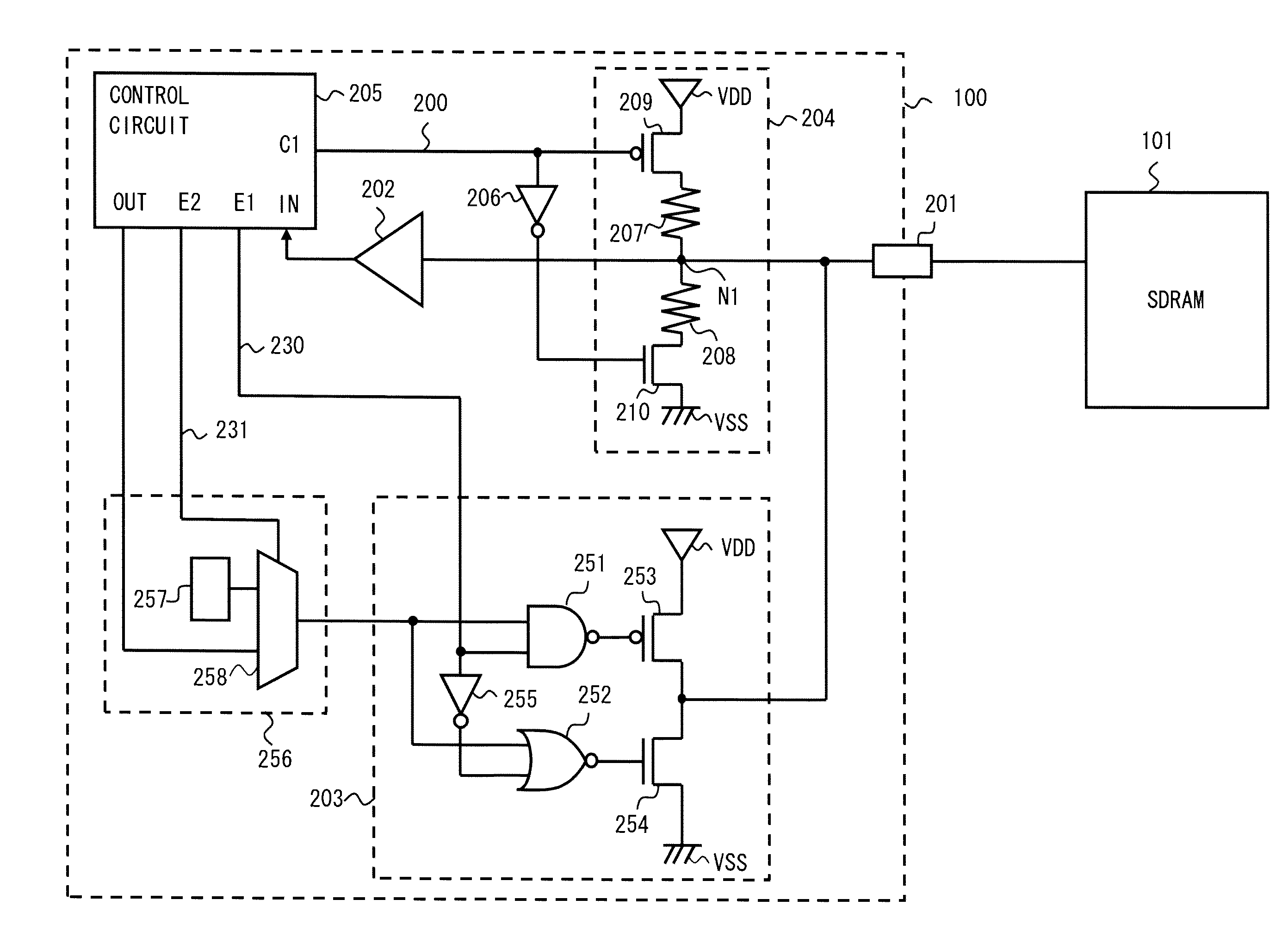
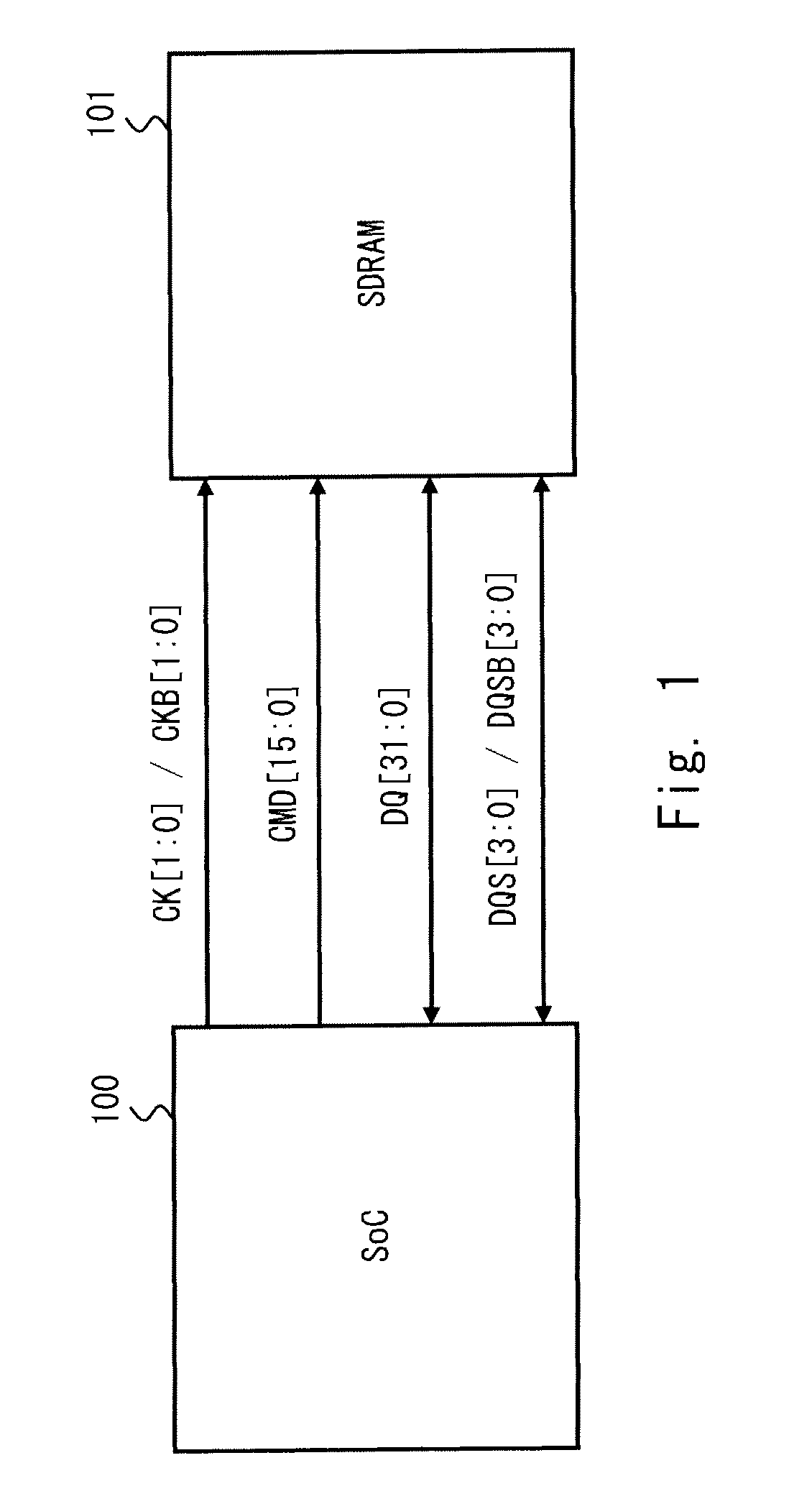
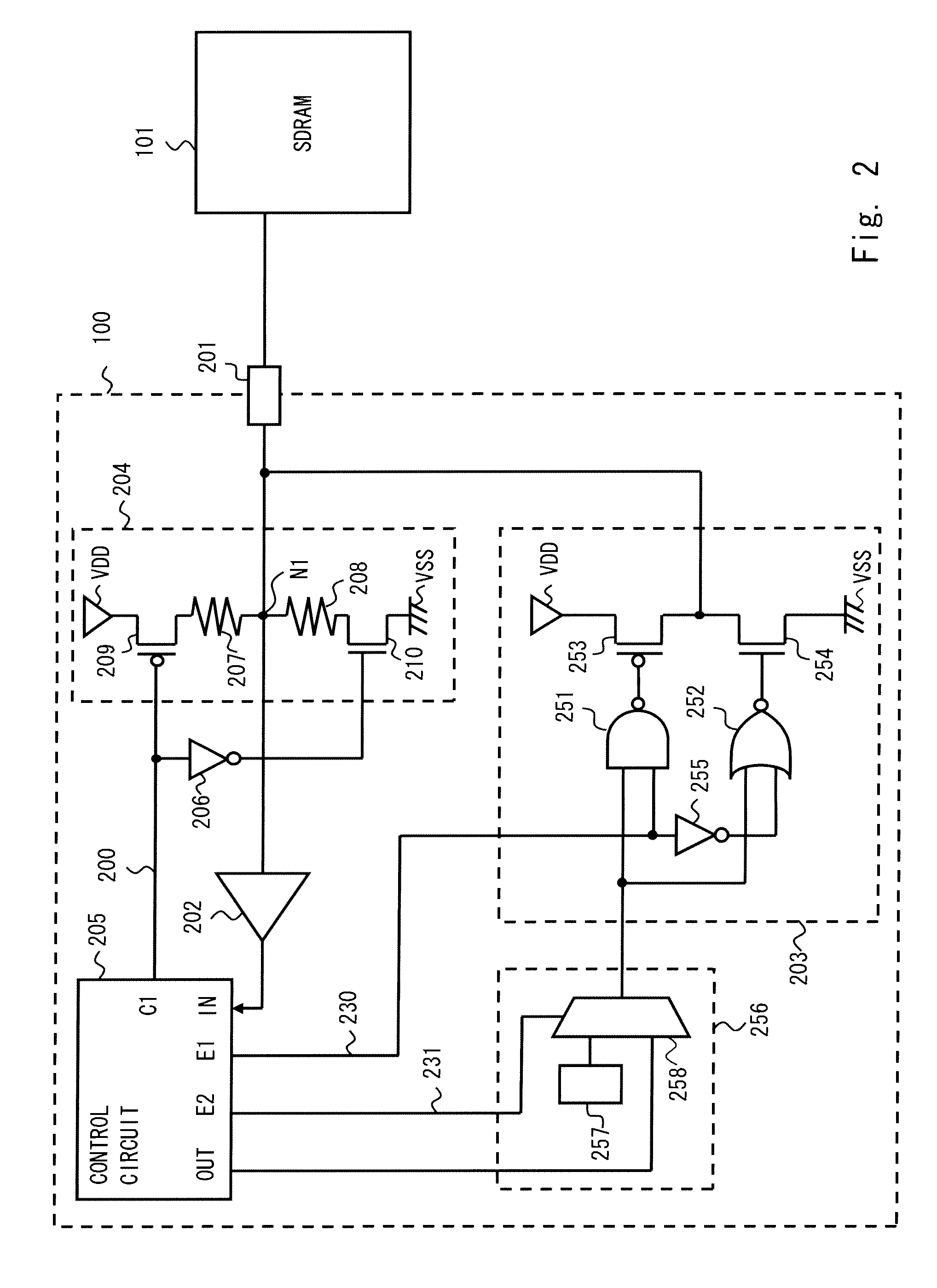
[0026]Referring to the drawings, a semiconductor integrated circuit according to a first exemplary embodiment of the present invention will be described. The present invention can be applied to a circuit which includes a data transmitting circuit that transmits data in parallel through a plurality of signal lines and a data receiving circuit that receives the data transmitted from the data transmitting circuit, and which controls the output of the data transmitting circuit based on a control signal. In this exemplary embodiment, a case is explained hereinafter in which the circuit shown in FIG. 1 includes an SoC (System on Chip) circuit and an SDRAM (Synchronous Dynamic Random Access Memory) circuit, and data transmission is executed between the SoC circuit and the SDRAM circuit through signal lines for bidirectionally transmitting data between these circuits (hereinafter, referred to simply as “bidirectional signal lines”).

[0027]FIG. 1 illustrates a semiconductor integrated circuit...


PUM


Abstract

Provided is a semiconductor integrated circuit according to an exemplary aspect of the present invention including a data transmitting circuit that transmits data in parallel through a plurality of signal lines and a data receiving circuit that receives the data. The data transmitting circuit includes a plurality of data output circuits that output the data in a data transmission mode or set an output to a high impedance state in a HiZ mode, a plurality of data selection circuits that select one of the data and fixed data and output the selected data to the data output circuits, and a control circuit that controls the data output circuits to output the fixed data during a period between a time when a mode is switched from the HiZ mode to the data transmission mode and a time when the data output circuits start to output the data.

Description

INCORPORATION BY REFERENCE[0001]This application is based upon and claims the benefit of priority from Japanese patent application No. 2009-207627, filed on Sep. 9, 2009, the disclosure of which is incorporated herein in its entirety by reference.BACKGROUND[0002]1. Field of the Invention[0003]The present invention relates to a semiconductor integrated circuit, and more particularly, to a semiconductor integrated circuit suitable for power-supply noise reduction.[0004]2. Description of Related Art[0005]In a semiconductor integrated circuit, there has been a problem that data transmission between a data transmitting circuit and a data receiving circuit is not accurately executed when power-supply noise occurs on a plurality of signal lines used for the data transmission between these circuits.[0006]Therefore, a countermeasure, for example, ODT (On Die Termination) technique has been provided to reduce the power-supply noise on signal lines used for data reception of the data receiving...

Claims


Application Information

Patent Timeline
Patent Type & Authority Patents(United States)
IPC IPC(8): H03K19/00H03K19/02
CPCG06F13/4072G11C7/1006G11C7/1051G11C7/1057G11C7/1066G11C7/1084G11C7/1093H03K19/0005G11C11/4096G11C7/22G11C7/1078G06F2213/0038Y02B60/1235Y02B60/1228Y02D10/00G11C11/4093
Inventor KOMYO, MASAYASUIIZUKA, YOICHI
Owner RENESAS ELECTRONICS CORP
Why Eureka
Try Eureka