Semiconductor device and fabrication method

a technology of semiconductor devices and fabrication methods, applied in semiconductor devices, semiconductor/solid-state device details, electrical apparatus, etc., can solve the problems of greater package warp and swelling, difficult to achieve two objects at the same time, and high assembly height of stacking package sip, etc., to achieve a lower assembly height and reduce warp.

Active Publication Date: 2011-08-23
GK BRIDGE 1
View PDF14 Cites 52 Cited by
  • Summary
  • Abstract
  • Description
  • Claims
  • Application Information

AI Technical Summary

Benefits of technology

[0016]An exemplary object of the present invention is to provide a semiconductor device that can simultaneously achieve a lower profile of assembly height and reduced warp and a method of fabricating such a semiconductor device.

Problems solved by technology

However, stacked-package SiP have the problem of higher assembly height than stacked-semiconductor element SiP in which a plurality of semiconductor elements are stacked in one package.
Stacked-package SiP further have the problems of greater package warp and swelling due to the thinning of the interposer substrate and partial molding in which only sites for mounting semiconductor elements are molded.
Although both lower profile of the assembly height and reduced warp of the package are sought in stacked-package SiP, these two objects are difficult to achieve simultaneously in stacked-package SiP.
However, such a package adopts a partially molded construction only for semiconductor elements, and as a result, warp is difficult to suppress at the ends of the package that are not sealed by molding.
However, the reverse surface of the semiconductor element is exposed by grinding, and although the thickness of the package can be reduced, warp in the region of the semiconductor element is difficult to suppress.
However, when reducing the thickness of a substrate to achieve assembly height of a lower profile, warp of the package is difficult to absorb by merely adjusting the height of electrodes.
Lower profile of the assembly height and reduced warp are therefore difficult to achieve simultaneously.

Method used


Image

  • Semiconductor device and fabrication method
  • Semiconductor device and fabrication method
  • Semiconductor device and fabrication method

Examples


first embodiment

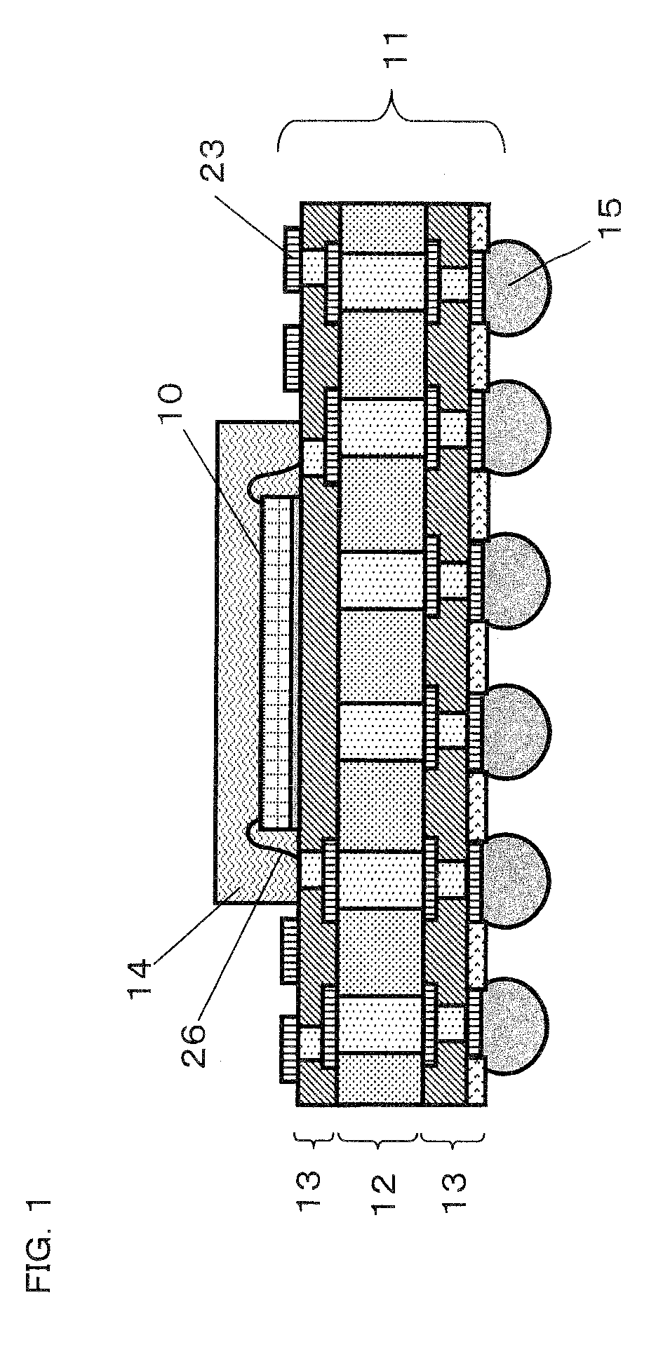
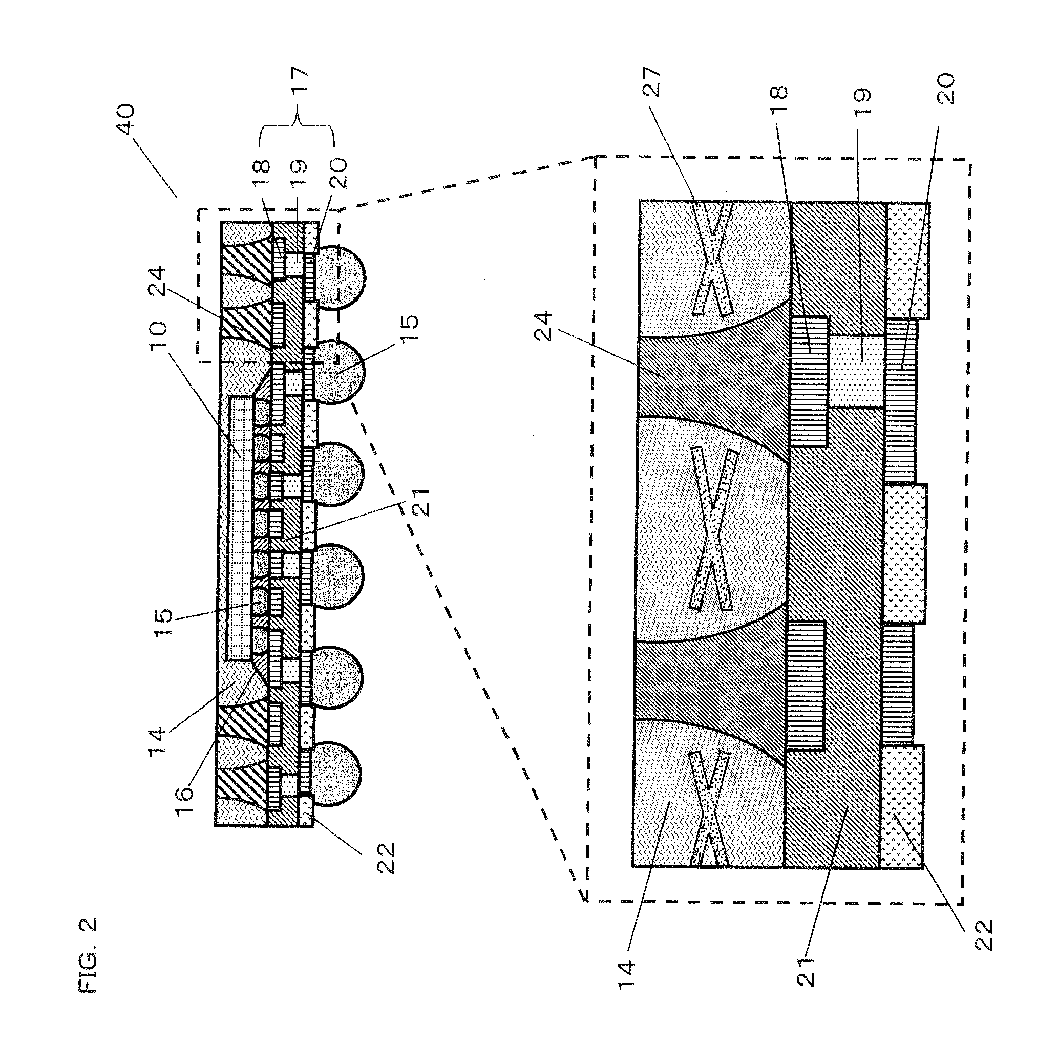
[0132]FIGS. 13A to 13L are sectional views showing the steps of a method of fabricating a semiconductor device according to the first exemplary embodiment of the present invention in order. This method is for fabricating a semiconductor device such as shown in FIG. 2.

[0133]First, as shown in FIG. 13A, metal body 33 is subjected to the processes of wet cleaning, dry cleaning, leveling, and roughening as necessary.

[0134]Metal body 33 is ultimately caused to function as metal posts 24. Consequently, at least one metal selected from the group of copper, aluminum, nickel, stainless steel, iron, magnesium, and zinc, or an alloy that takes these metals as principal components is used as metal body 33. The selection of copper as metal body 33 is particularly desirable according to the standpoints of electrical resistance and cost. Copper is used in the present embodiment.

[0135]Next, as shown in FIG. 13B, lower-layer wiring 18 is formed on metal body 33 by means of, for example, a subtracti...

second embodiment

[0187]FIG. 17 is a sectional view showing a portion of the method of fabricating the semiconductor device according to the second exemplary embodiment of the present invention. The fabrication method of the present embodiment is for fabricating the semiconductor device of the second embodiment such as shown in FIG. 6.

[0188]The following explanation regards portions that differ from the first exemplary embodiment of the method of fabricating a semiconductor device. Parts that are not specifically described are the same as in the explanation of the first exemplary embodiment of the method of fabricating a semiconductor device.

[0189]Explanation first regards the method of stacking sealing layer 14.

[0190]As shown in FIG. 17, semiconductor element area opening 36 and metal post area openings 37 are provided in sealing layer 14 in advance. The openings are formed using, for example, a laser, drill, dry etching, and wet etching. In the present embodiment, a laser is used.

[0191]Next, as sho...


PUM


Abstract

A semiconductor device, in which a semiconductor element is mounted on one side of a circuit board that is made up from an insulating layer and a wiring layer, includes metal posts provided on the side of the circuit board on which the semiconductor element is mounted; and a sealing layer provided on the side of the circuit board on which the semiconductor element is mounted such that the semiconductor element is covered and such that only portions of the metal posts are exposed.

Description

[0001]This application is based upon and claims the benefit of priority from Japanese patent application No. 2007-105852, filed on Apr. 13, 2007, the disclosure of which is incorporated herein in its entirety by reference.BACKGROUND OF THE INVENTION[0002]1. Field of the Invention[0003]The present invention relates to a semiconductor device for realizing a package for stacked package SiP that is thinner and less prone to warp, and to a method of fabricating such a semiconductor device.[0004]2. Description of the Related Art[0005]SiP (System in Package) is receiving attention as a technology for achieving smaller electronic apparatuses having higher functionality. Within SiP, stacked-package SiP (PoP, Package on Package) provides an easy solution to the problem of ensuring that products are defect-free. In addition, stacked-package SiP allows a high degree of freedom in combining chips. As a result, orders for stacked-package SiP are increasing, particularly for portable telephones.[0...

Claims


Application Information

Patent Timeline
Patent Type & Authority Patents(United States)
IPC IPC(8): H01L23/02
CPCH01L21/4853H01L21/4857H01L21/6835H01L23/295H01L23/3128H01L23/3135H01L25/105H01L23/49816H01L23/5389H01L24/16H01L24/81H01L24/85H01L2221/68345H01L2221/68377H01L2224/114H01L2224/116H01L2224/16225H01L2224/32225H01L2224/48091H01L2224/48225H01L2224/48227H01L2224/48235H01L2224/73204H01L2224/73253H01L2224/73265H01L2224/81801H01L2225/1058H01L2924/01012H01L2924/01046H01L2924/01057H01L2924/01078H01L2924/01079H01L2924/15153H01L2924/1517H01L2924/15311H01L2924/15331H01L2924/19041H01L24/48H01L2924/01019H01L2924/01322H01L2224/85H01L2924/3511H01L2225/1023H01L2224/16235H01L2924/00014H01L2924/00H01L2924/00012H01L2924/181H01L24/73H01L2924/00011H01L2224/0401H01L2224/45099H01L2224/45015H01L2924/207
Inventor MORI, KENTAROKIKUCHI, KATSUMIYAMAMICHI, SHINTARO
Owner GK BRIDGE 1
Why Eureka
Try Eureka