Optical clock signal distribution using through-silicon vias

a silicon via and clock signal technology, applied in the field of optical signals, can solve the problems of preventing efficient allocation of optical detectors, affecting the efficiency of optical detection, and consuming more power, so as to reduce the heat generated by clock circuits and reduce the attenuation of ligh

Inactive Publication Date: 2011-08-23
TAIWAN SEMICON MFG CO LTD
View PDF9 Cites 5 Cited by
  • Summary
  • Abstract
  • Description
  • Claims
  • Application Information

AI Technical Summary

Benefits of technology

The advantageous features of the present invention include reduced heat generated by clock circuits, reduced attenuation of the light carrying the optical clock signals, and the elimination of the requirement for re-routing metallization layers for the clock circuits.

Problems solved by technology

Significantly greater power consumption and more severe heat-dissipating problems are hence resulted.
The conventional methods, however, suffer from drawbacks.
For example, if the optical signal is introduced into substrates from the front sides of the respective semiconductor chips, then the metallization layers, which already have high densities, will prevent efficient allocation of optical detectors.
Therefore, the cost and manufacturing complexity increase.

Method used


Image

  • Optical clock signal distribution using through-silicon vias
  • Optical clock signal distribution using through-silicon vias
  • Optical clock signal distribution using through-silicon vias

Examples


Embodiment Construction

The making and using of the presently preferred embodiments are discussed in detail below. It should be appreciated, however, that the present invention provides many applicable inventive concepts that can be embodied in a wide variety of specific contexts. The specific embodiments discussed are merely illustrative of specific ways to make and use the invention, and do not limit the scope of the invention.

A novel integrated circuit structure for receiving optical clock signals and converting the optical clock signals to electrical clock signals is provided. The variations and the operation of the preferred embodiments are discussed. Throughout the various views and illustrative embodiments of the present invention, like reference numbers are used to designate like elements.

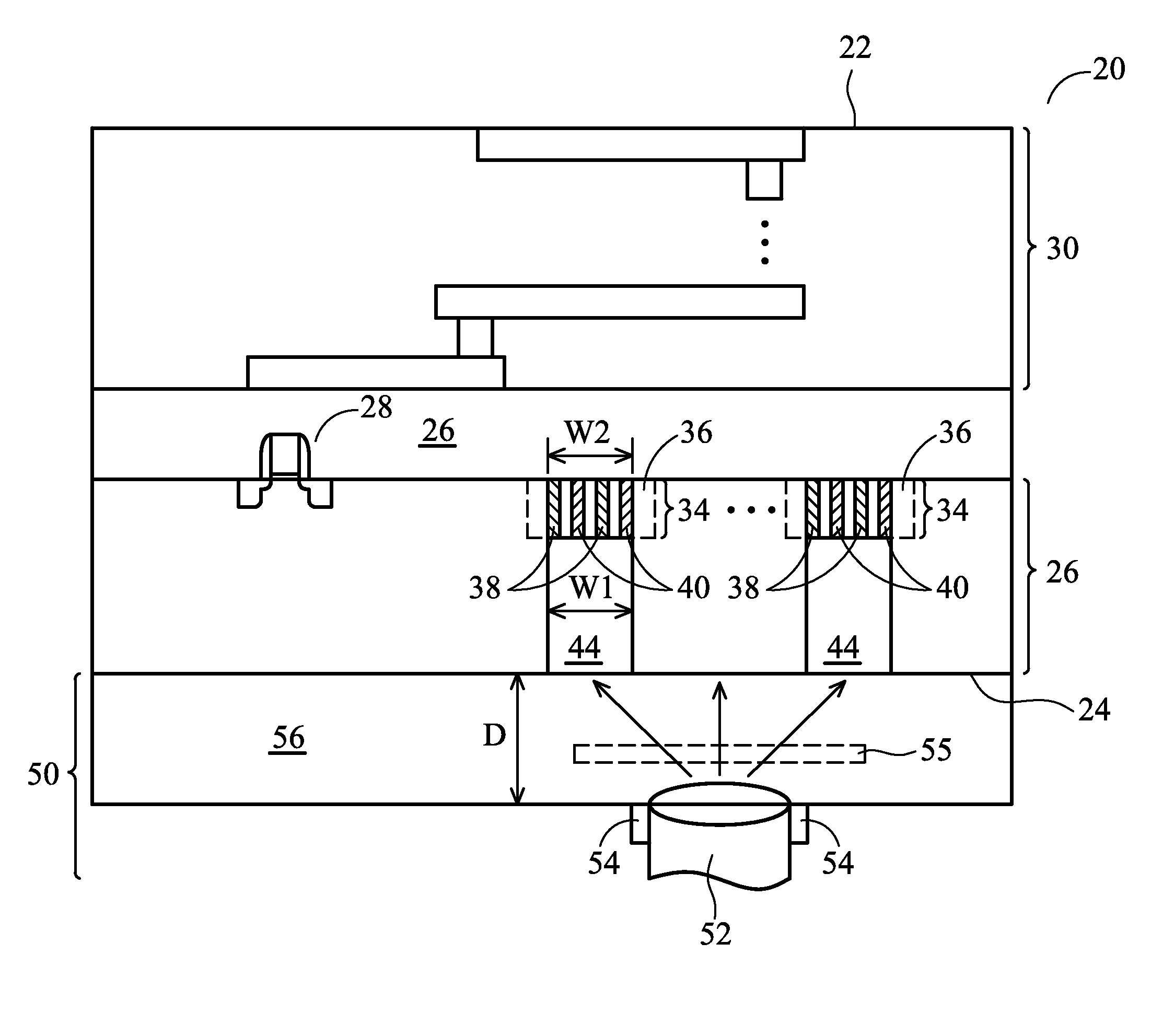
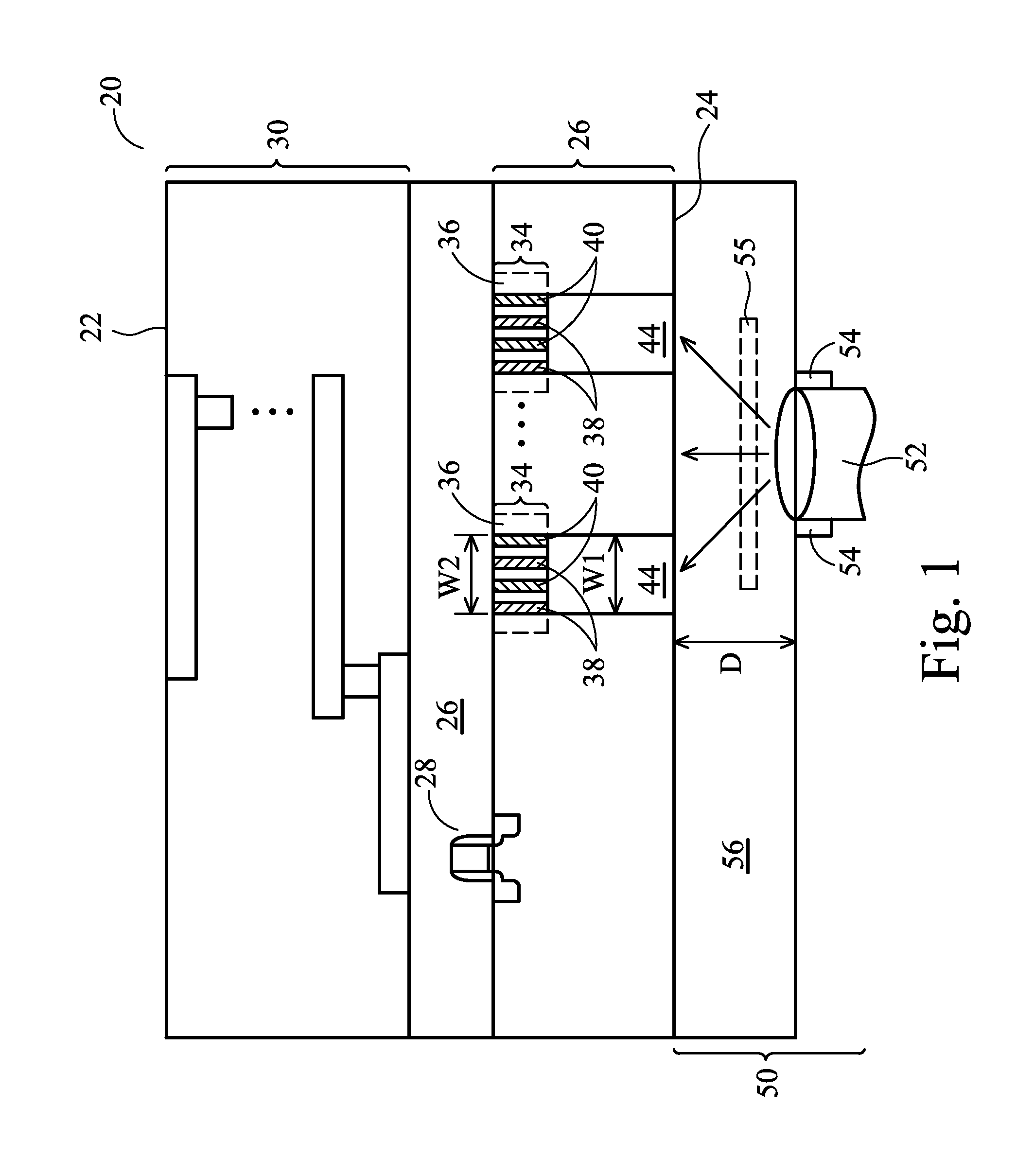
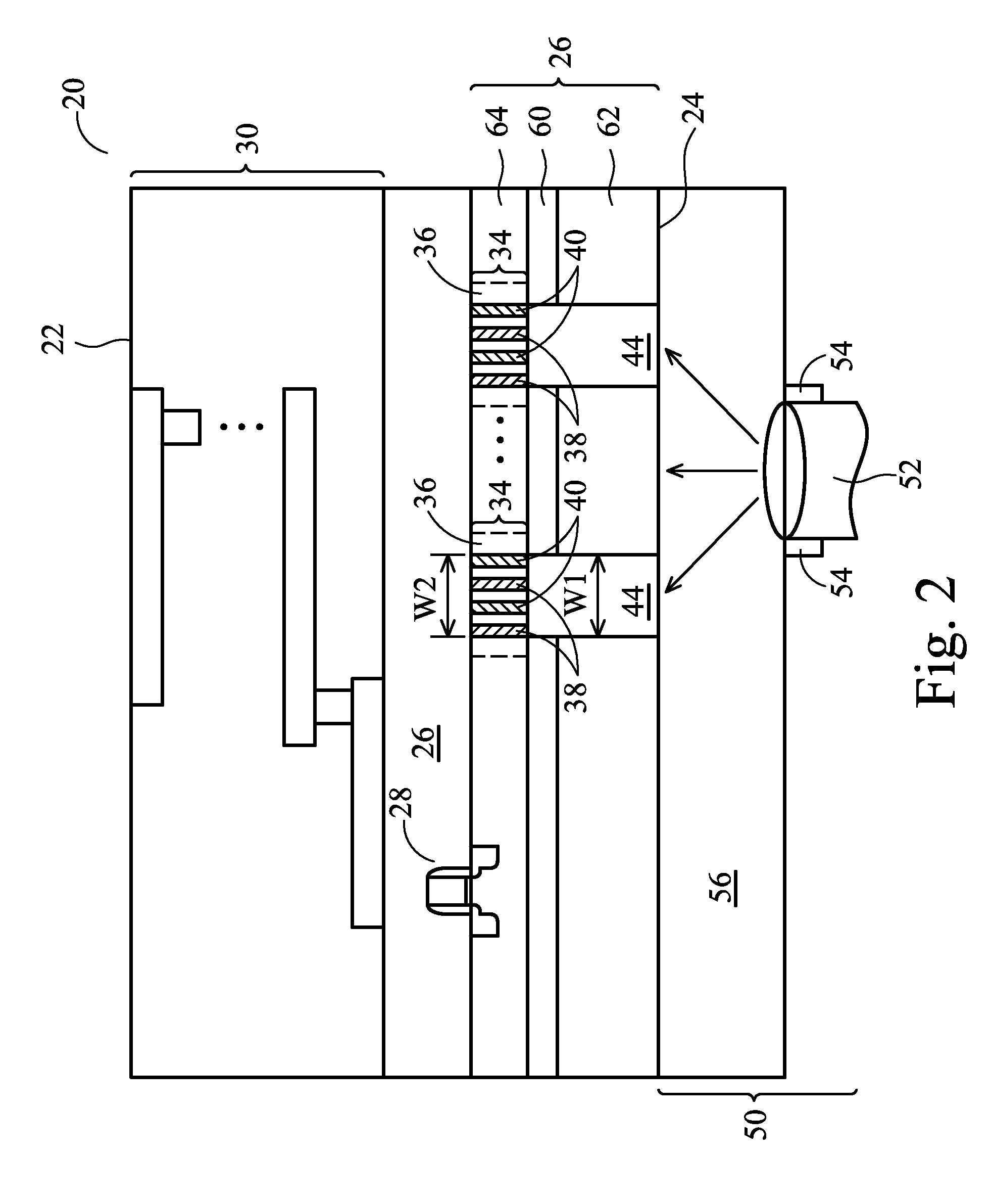
FIG. 1 illustrates a cross-sectional view of an embodiment of the present invention, which includes chip 20. Chip 20 has front surface 22 and back surface 24. Semiconductor substrate 26 is inside chip 20. In an em...


PUM


Abstract

An integrated circuit structure includes a semiconductor chip including a front surface and a back surface; a via extending from the back surface of the semiconductor chip into the semiconductor chip, wherein the via is light transparent; and a photon detector in the semiconductor chip and exposed to the via.

Description

TECHNICAL FIELDThis invention relates generally to optical signals for an integrated circuit, and more particularly to semiconductor chips having built-in circuits for converting optical clock signals to electrical clock signals.BACKGROUNDClock signals are essential to the operation of modern integrated circuits, in which the operations are synchronized by clock signals, which often contains a repeated pattern of “1010.” To speed up the integrated circuits, the clock signals have to be speed up. Currently, the clock signals have the frequencies in giga hertz (GHz) ranges. It is expected that by year 2010, the clock signals will be in the range of about 15 to 20 GHz. In this range, the electrical signal begins to merge with optical signals.With the increase in the frequencies of clock signals, more heat is generated by the clock signal circuits, for example, flip-flops. Significantly greater power consumption and more severe heat-dissipating problems are hence resulted. With the incr...

Claims


Application Information

Patent Timeline
Patent Type & Authority Patents(United States)
IPC IPC(8): G02B6/12
CPCG02B6/43G06F1/105
Inventor CHANG, SHIH-CHENGLIN, JIN-LIENHSU, KUO-CHINGCHING, KAI-MINGWU, JIUN YICHEN, YEN-HUEI
Owner TAIWAN SEMICON MFG CO LTD
Why Eureka
Try Eureka