
Magnetic sensing element and method for manufacturing the same

a technology manufacturing method, which is applied in the field of magnetic sensing element, can solve the problems of not being able to improve, especially, and achieve the effect of increasing recording density and reducing reproducing

Active Publication Date: 2011-08-30
TDK CORPARATION
View PDF5 Cites 8 Cited by
  • Summary
  • Abstract
  • Description
  • Claims
  • Application Information

AI Technical Summary

Benefits of technology

The present invention provides a magnetic sensing element with improved performance. Specifically, the invention improves the half-amplitude pulse width (PW50) and signal-to-noise ratio (SN ratio) without compromising reproducing characteristics such as resistance to change in resistance (Δ R / R). This is achieved by improving the underlying layer, which is in contact with the lower shield layer and is composed of an amorphous magnetic material. The invention also maintains good planarizability and stability of the underlying layer, which helps to maintain the rate of change in resistance (Δ R / R) at the same level as before. The invention provides a method for manufacturing the magnetic sensing element with the described improvements.

Problems solved by technology

In the prior art, however, no improvement has been made, particularly, on the underlying layer, which is to be disposed in contact with the lower shield layer, so as to facilitate narrowing the gap without deteriorating reproducing characteristics.

Method used


Image

  • Magnetic sensing element and method for manufacturing the same
  • Magnetic sensing element and method for manufacturing the same
  • Magnetic sensing element and method for manufacturing the same

Examples


examples 1 to 5

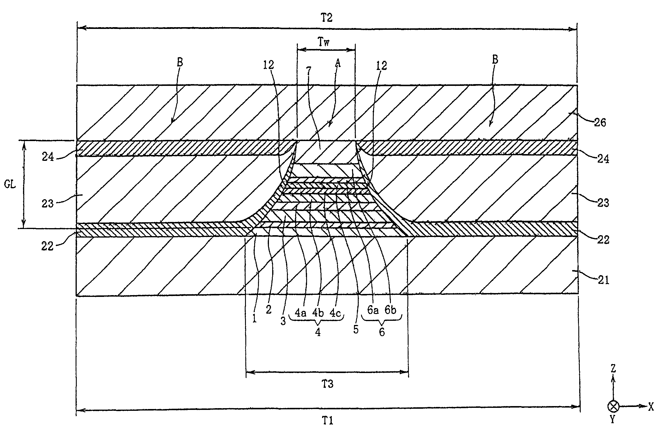
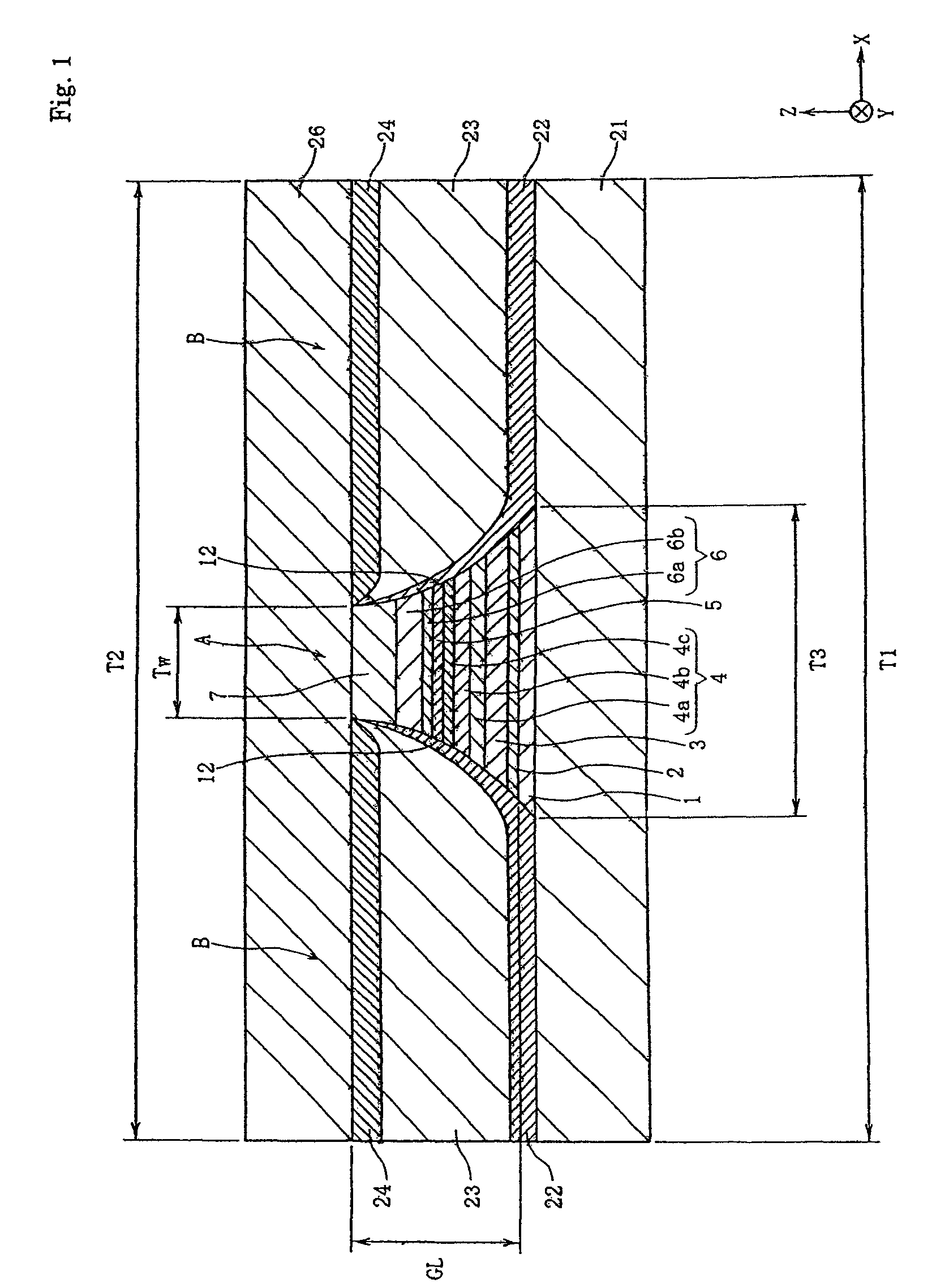
[0134]A tunneling magnetic sensing element shown in FIG. 1 was fabricated.

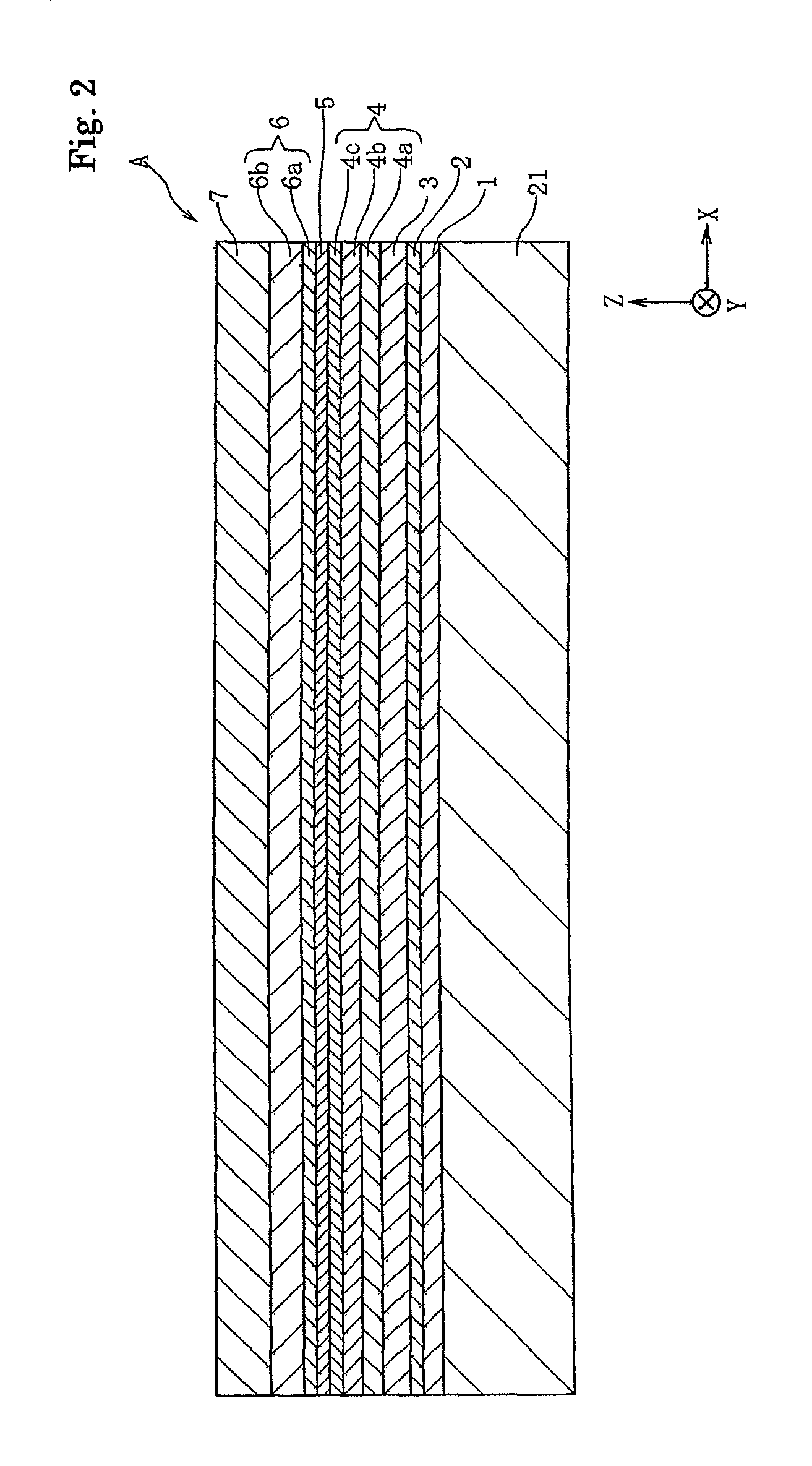
[0135]A multilayered film A was formed by depositing underlying layer 1; {Co0.75Fe0.25}80at %B20at %(X) / seed layer 2; Ru(30) / antiferromagnetic layer 3; Ir26at %Mn74at %(70) / pinned magnetic layer 4 [first pinned magnetic sublayer 4a; Co70at %Fe30at %(21) / nonmagnetic intermediate sublayer 4b; Ru(8.5) / second pinned magnetic sublayer 4c; {Co50Fe50}80at %B20at %(19)] / insulating barrier layer 5 / free magnetic layer 6 [enhancement layer 6a; Co20at %Fe80at %(10) / soft magnetic layer 6b; Ni88at %Fe12at %(50)] / protective layer 7; [Ru(20) / Ta(270)] in that order from the bottom.

[0136]In the multilayered film A, each of the values in parentheses indicates an average film thickness in terms of Å.

[0137]In the experiment, the insulating barrier layer 5 was composed of Al—O in such a manner that an Al layer was first deposited on the second pinned magnetic sublayer 4c with an average film thickness of 4.3 Å and then oxidized.

[01...

example 1

Conventional Example 1

[0140]A sample having the same film composition as the above multilayered film A was prepared except that the underlying layer 1 was replaced with a layer of Ta(30).

[0141]After subjected to the same annealing treatment in a magnetic field as the samples of Examples, the sample of Conventional Example 1 was measured for film properties such as rate of change in resistance (Δ R / R) and electric properties such as PW50.

example 2

Conventional Example 2

[0142]A sample having the same film composition as the above multilayered film A was prepared except that the underlying layer 1 was not provided.

[0143]After subjected to the same annealing treatment in a magnetic field as the samples of Examples, the sample of Conventional Example 2 was measured for film properties such as rate of change in resistance (Δ R / R).

[0144]The experimental results are shown in Table 1 below.

[0145]

TABLE 1Film propertiesElectric propertiesTuMRRAΔSNUnderlying layerTotal(ΩR / RHex*HexratioPW50Res.Sample(Å)thickness (Å)μm2)(%)(Oe)(Oe)(dB)(nm)(%)Con.Ta(30)5653.5431.03800290014.0270.2266.02Ex. 1Con.—5353.5030.829802650———Ex. 2Ex. 1(Co75Fe25)80B20(10)5453.4830.234002720———Ex. 2(Co75Fe25)80B20(20)5553.4230.83820294014.2868.2568.22Ex. 3(Co75Fe25)80B20(30)5653.4430.83800290014.3068.2167.85Ex. 4(Co75Fe25)80B20(50)5853.4230.53800288014.2268.3267.92Ex. 5(Co75Fe25)80B20(100)5353.4230.23820292014.0269.3666.5 

[0146]Hex shown in Table 1 indicates a magni...


PUM

PropertyMeasurementUnit
width Twaaaaaaaaaa
coercive force Hcaaaaaaaaaa
thicknessaaaaaaaaaa

Abstract

An underlying layer is composed of Co—Fe—B that is an amorphous magnetic material. Thus, the upper surface of the underlying layer can be taken as a lower shield layer-side reference position for obtaining a gap length (GL) between upper and lower shields, resulting in a narrower gap than before. In addition, since the underlying layer has an amorphous structure, the underlying layer does not adversely affect the crystalline orientation of individual layers to be formed thereon, and the surface of the underlying layer has good planarizability. Accordingly, PW50 (half-amplitude pulse width) and SN ratio can be improved more than before without causing a decrease in rate of change in resistance (Δ R / R) or the like, thereby achieving a structure suitable for increasing recording density.

Description

CLAIM OF PRIORITY[0001]This application claims benefit of the Japanese Patent Application No. 2007-128827 filed on May 15, 2007, the entire content of which is hereby incorporated by reference.BACKGROUND[0002]1. Field of the Invention[0003]Particularly, the present invention relates to a magnetic sensing element in which PW50 (half-amplitude pulse width) and SN ratio (Signal to Noise Ratio) are improved more than before without causing a decrease in reproducing characteristics such as rate of change in resistance (Δ R / R) and which is thus suitable for increasing recording density, and a method for manufacturing the same.[0004]2. Description of the Related Art[0005]Typically, tunneling magnetoresistive elements have such a structure that a multilayered film, which makes use of a tunneling magnetoresistance effect, is interposed between lower and upper shied layers that are opposed to each other in a film thickness direction.[0006]More specifically, the multilayered film is formed by ...

Claims


Application Information

Patent Timeline
Patent Type & Authority Patents(United States)
IPC IPC(8): G11B5/33
CPCB82Y10/00B82Y25/00B82Y40/00G01R33/093G11B5/3909H01F10/30H01F41/302H01L43/08H01L43/12G11B5/3906H01F10/3254H01F10/3277H10N50/10H10N50/01
Inventor TANAKA, KENICHIUMETSU, EIJIIKARASHI, KAZUAKIASATSUMA, KOTAOKANISHI, NORIMASANISHIYAMA, YOSHIHIROSAITO, MASAMICHIIDE, YOSUKENISHIMURA, KAZUMASANAKABAYASHI, RYOKOBAYASHI, HIDEKAZUHANADA, AKIOHASEGAWA, NAOYA
Owner TDK CORPARATION
Learn More