Magnetic sensing element and method for manufacturing the same
- Summary
- Abstract
- Description
- Claims
- Application Information
AI Technical Summary
Benefits of technology
Problems solved by technology
Method used
Image
Examples
examples 1 to 5
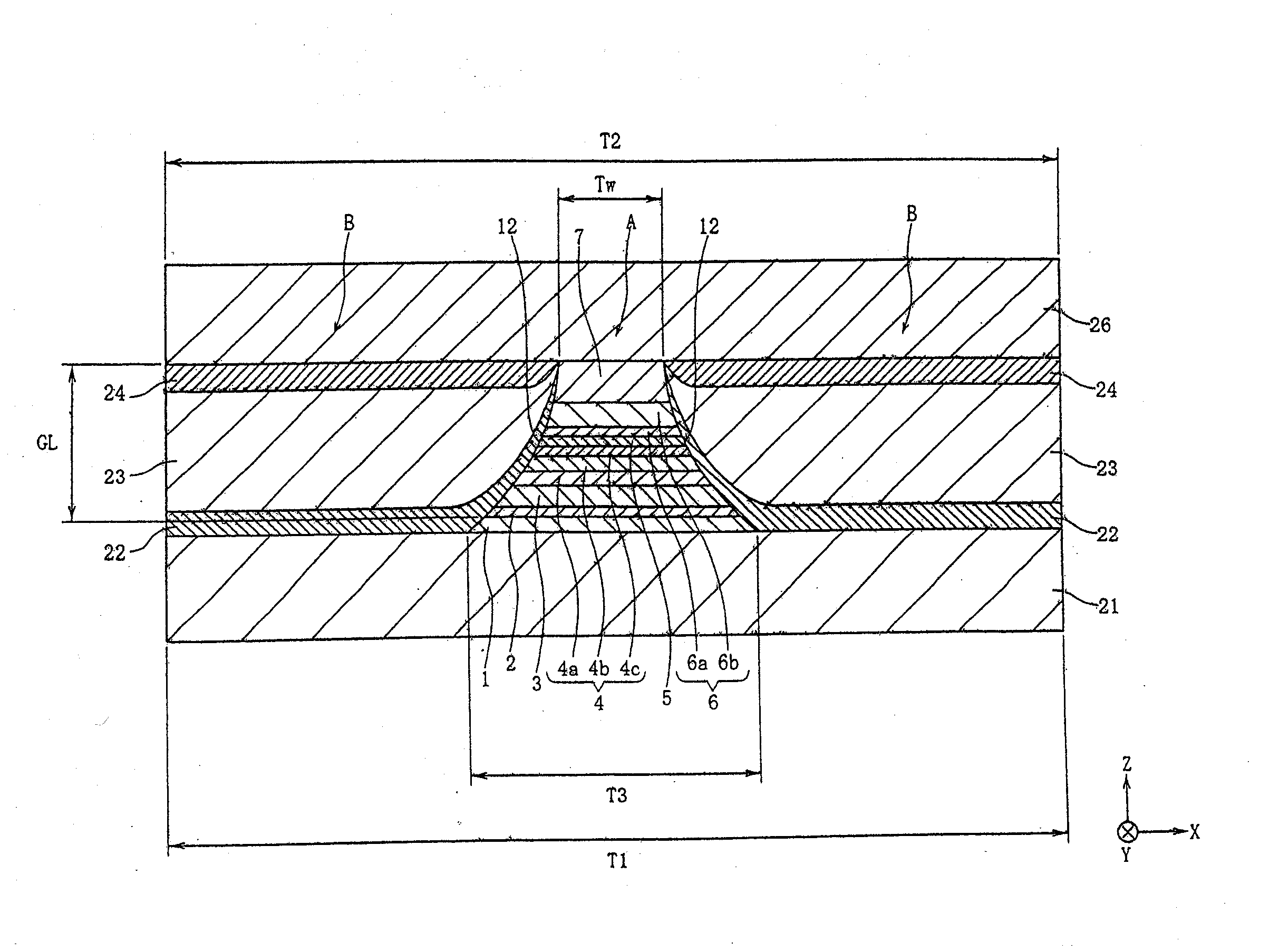
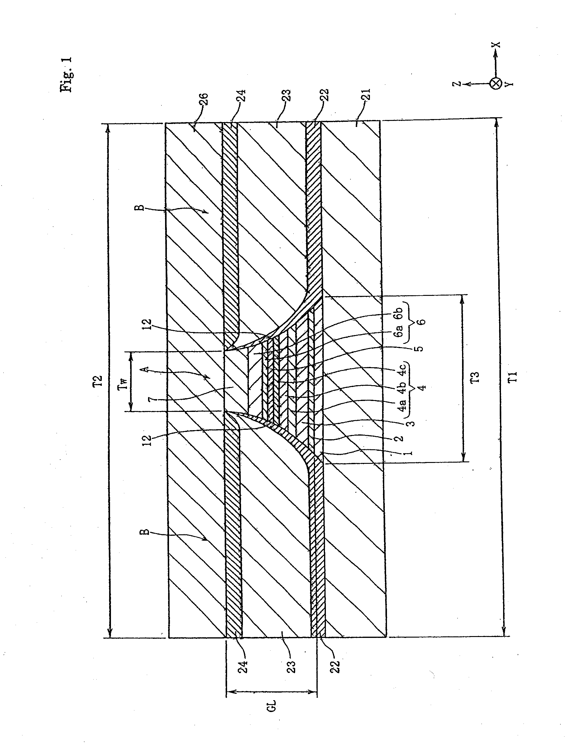
[0134]A tunneling magnetic sensing element shown in FIG. 1 was fabricated.
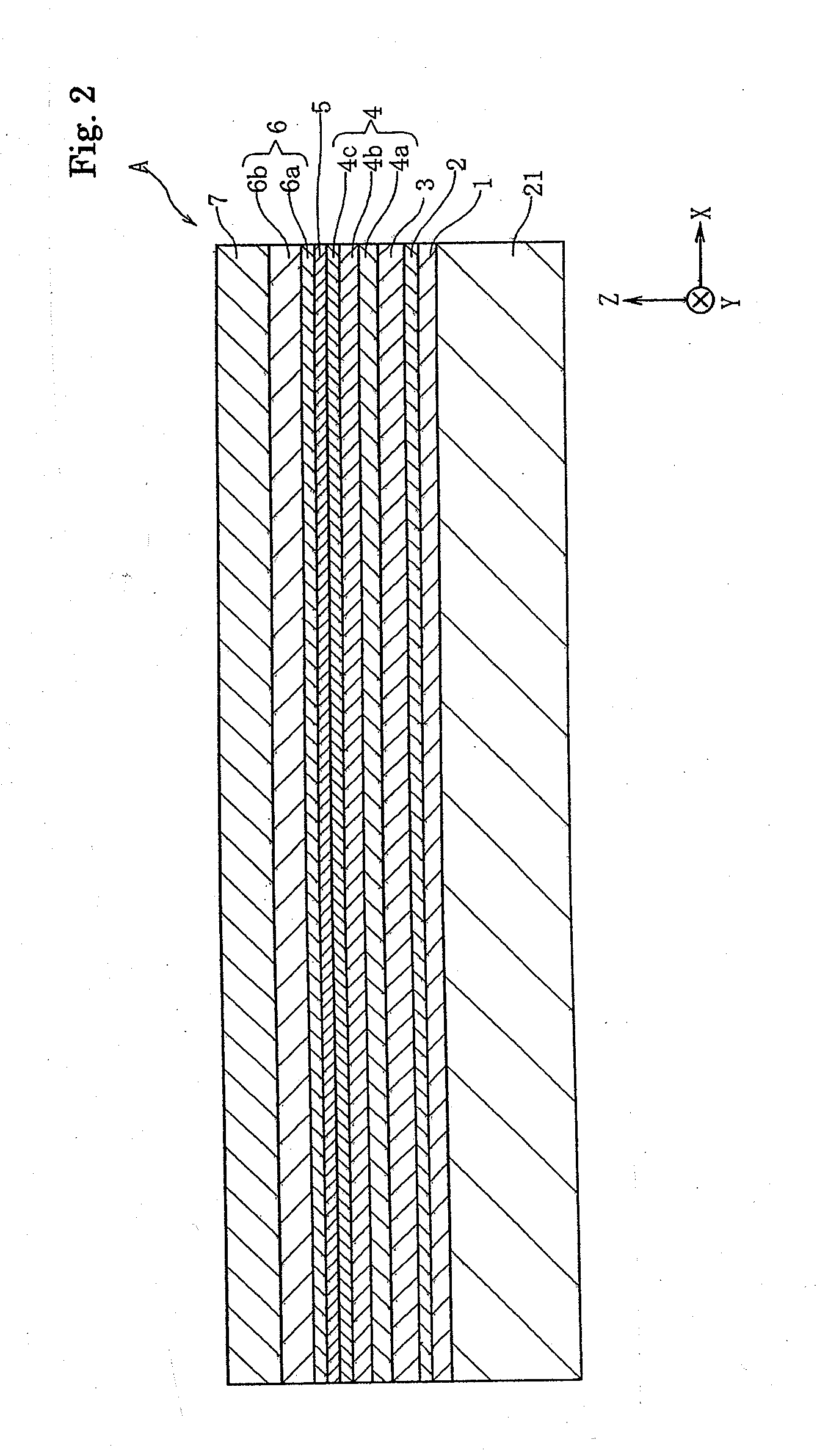
[0135]A multilayered film A was formed by depositing underlying layer 1; {Co0.75Fe0.25}80at%B20at%(X) / seed layer 2; Ru(30) / antiferromagnetic layer 3; Ir26at%Mn74at%(70) / pinned magnetic layer 4 [first pinned magnetic sublayer 4a; Co70at%Fe30at%(21) / nonmagnetic intermediate sublayer 4b; Ru(8.5) / second pinned magnetic sublayer 4c; {Co50Fe50}80at%B20at%(19)] / insulating barrier layer 5 / free magnetic layer 6 [enhancement layer 6a; Co20at%Fe80at%(10) / soft magnetic layer 6b; Ni88at%Fe12at%(50)] / protective layer 7; [Ru(20) / Ta(270)] in that order from the bottom.
[0136]In the multilayered film A, each of the values in parentheses indicates an average film thickness in terms of Å.
[0137]In the experiment, the insulating barrier layer 5 was composed of Al—O in such a manner that an Al layer was first deposited on the second pinned magnetic sublayer 4c with an average film thickness of 4.3 Å and then oxidized.
[0138]After the...
example 1
Conventional Example 1
[0140]A sample having the same film composition as the above multilayered film A was prepared except that the underlying layer 1 was replaced with a layer of Ta(30).
[0141]After subjected to the same annealing treatment in a magnetic field as the samples of Examples, the sample of Conventional Example 1 was measured for film properties such as rate of change in resistance (Δ R / R) and electric properties such as PW50.
example 2
Conventional Example 2
[0142]A sample having the same film composition as the above multilayered film A was prepared except that the underlying layer 1 was not provided.
[0143]After subjected to the same annealing treatment in a magnetic field as the samples of Examples, the sample of Conventional Example 2 was measured for film properties such as rate of change in resistance (Δ R / R).
[0144]The experimental results are shown in Table 1 below.
TABLE 1Film propertiesElectric propertiesTuMRRAΔSNUnderlying layerTotal(ΩR / RHex*HexratioPW50Res.Sample(Å)thickness (Å)μm2)(%)(Oe)(Oe)(dB)(nm)(%)Con.Ta(30)5653.5431.03800290014.0270.2266.02Ex. 1Con.—5353.5030.829802650———Ex. 2Ex. 1(Co75Fe25)80B20(10)5453.4830.234002720———Ex. 2(Co75Fe25)80B20(20)5553.4230.83820294014.2868.2568.22Ex. 3(Co75Fe25)80B20(30)5653.4430.83800290014.3068.2167.85Ex. 4(Co75Fe25)80B20(50)5853.4230.53800288014.2268.3267.92Ex. 5(Co75Fe25)80B20(100)5353.4230.23820292014.0269.3666.5
[0145]Hex shown in Table 1 indicates a magnitude o...
PUM
 Abstract
Description
Claims
Application Information


