Circuit for high speed dynamic memory

a high-speed, dynamic memory technology, applied in the direction of information storage, static storage, digital storage, etc., can solve the problems of longening the time required for each read cycle, reads of memory cells to be destructive, and reads are destructive, so as to improve the operation of sense amplifiers and high-speed sense amplifier operations.

Inactive Publication Date: 2011-08-30
TAIWAN SEMICON MFG CO LTD
View PDF9 Cites 16 Cited by
  • Summary
  • Abstract
  • Description
  • Claims
  • Application Information

AI Technical Summary

Benefits of technology

[0007]These and other problems are generally solved or circumvented, and technical advantages are generally achieved, by embodiments of the present invention, which provides circuits and methods to improve the operation of sense amplifiers and the voltage references used with the sense amplifiers without requiring a dummy cells or added write select signals to enable high speed sense amplifier operations.

Problems solved by technology

The memory cell must be “written back” to restore the small stored charge at the end of each read cycle, because the storage capacitor discharges onto the bit line, the read is a destructive read out.
The charge sharing mechanism used by conventional DRAM cell accesses causes reads of the memory cell to be destructive, and requires a write back cycle after a read, lengthening the time required for each read cycle.

Method used


Image

  • Circuit for high speed dynamic memory
  • Circuit for high speed dynamic memory
  • Circuit for high speed dynamic memory

Examples


Embodiment Construction

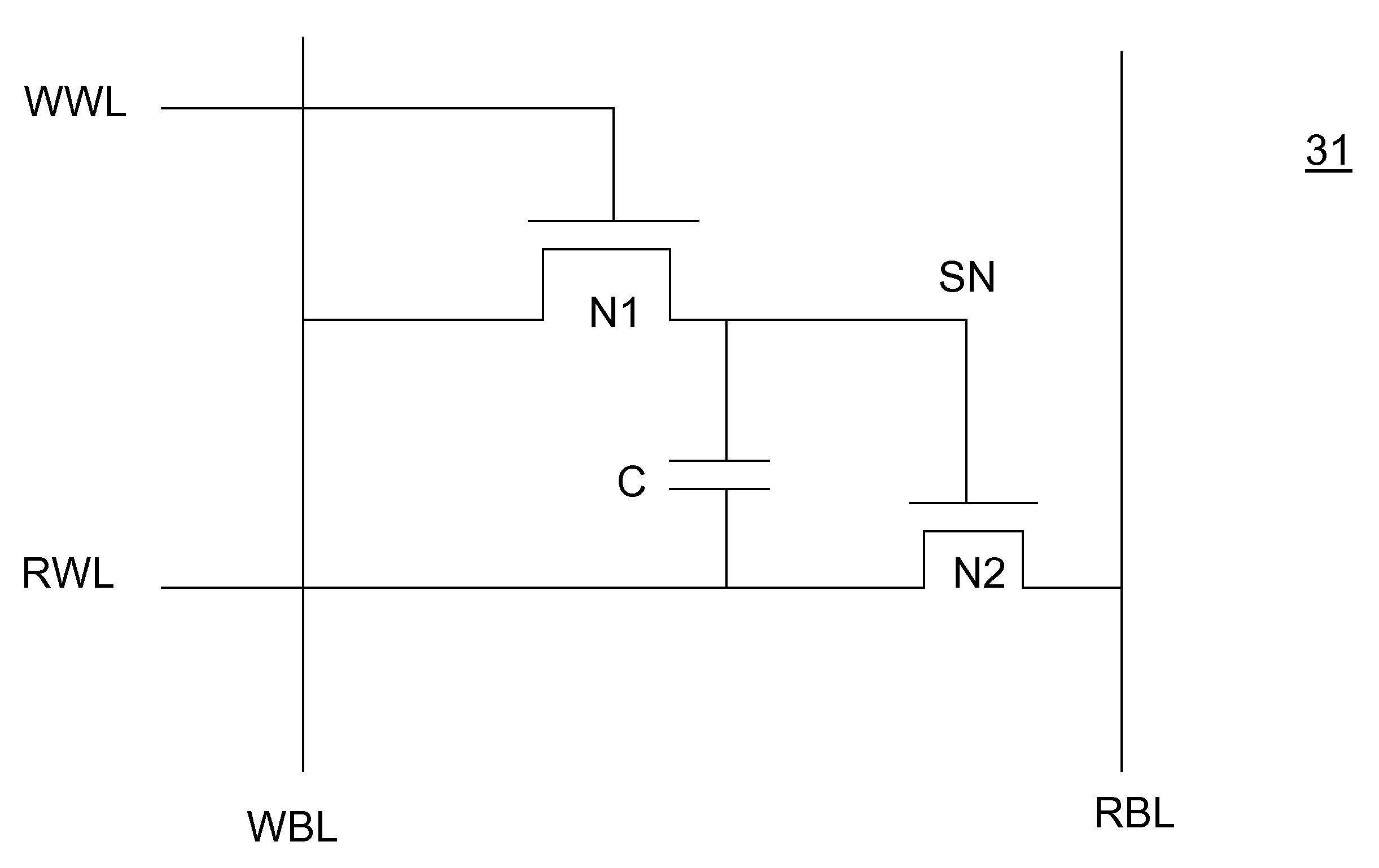
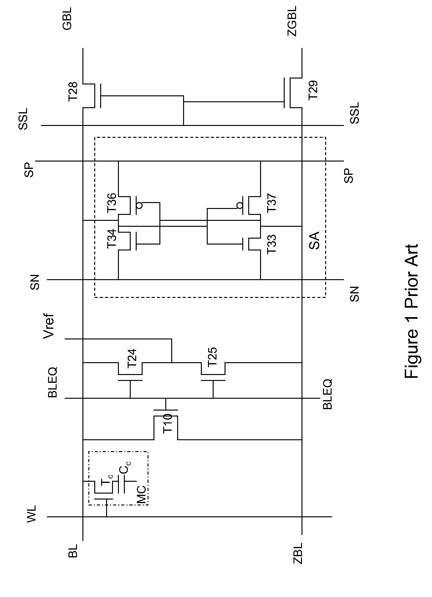
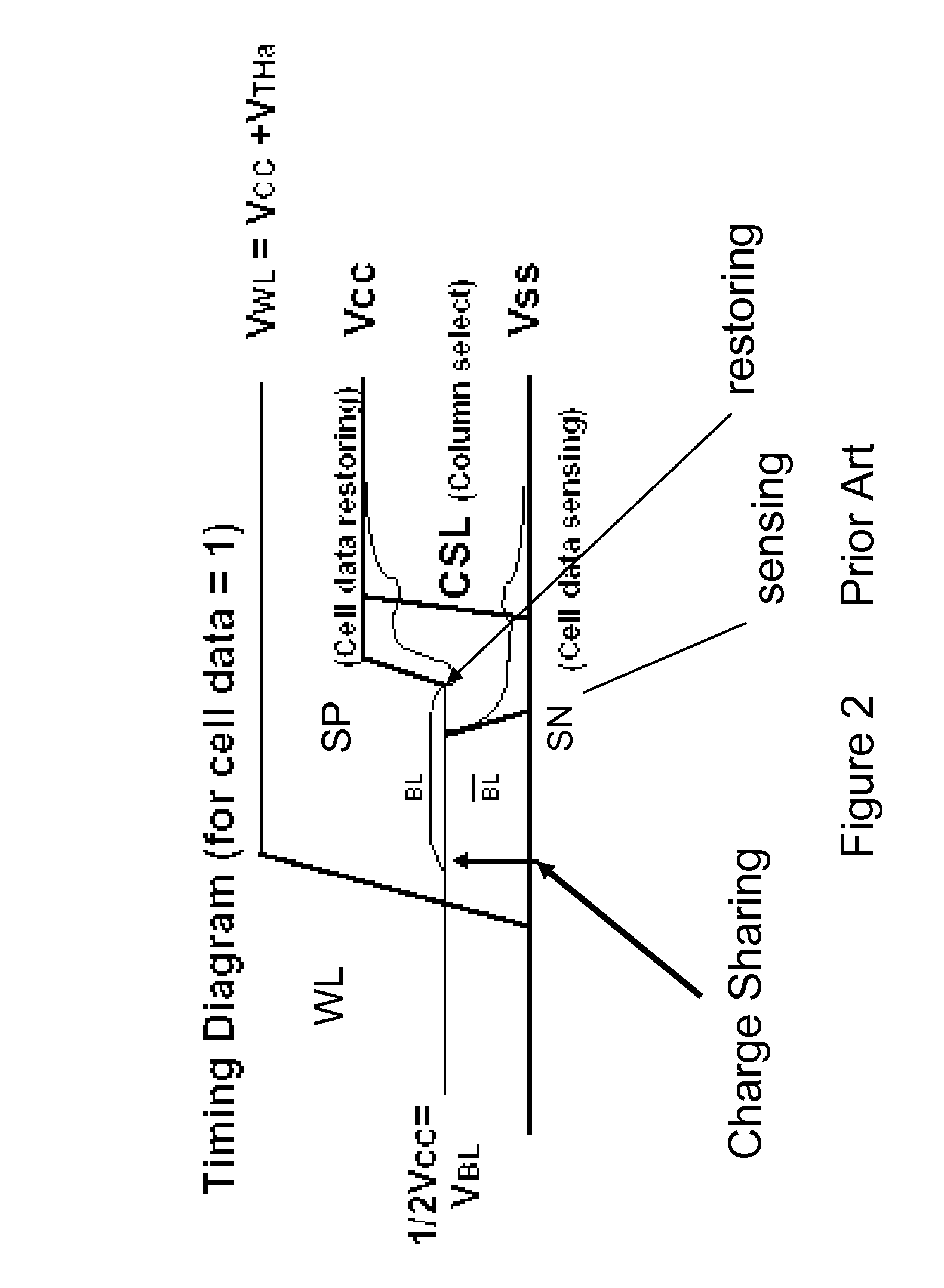
[0020]FIG. 1 depicts a small portion of a typical dynamic memory circuit of the prior art. Any read of a conventional dynamic memory cell such as the 1T1C cell MC in FIG. 1 is destructive, so the cell is always restored or rewritten at the end of the cycle. A “write” is simply a read cycle with write data impressed on the respective local bit line during the “restore” portion of the cycle. For a write, the read data is replaced or overwritten with the new write data and then written into the cell. Refresh cycles are also performed periodically to overcome loss of charge due to leakage.

[0021]In FIG. 1, memory cell MC is coupled at an intersection between a row or word line WL and a column or bit line BL. Although only one memory cell MC is depicted, another cell will be placed at the intersection of each of a plurality of word lines WL and the bit line BL. Similarly, a plurality of memory cells will also be placed at the intersections of each of a plurality of row lines WL (only one ...


PUM


Abstract

A memory cell includes a write access transistor coupled between a storage node and a write bit line, and active during a write cycle responsive to a voltage on a write word line; a read access transistor coupled between a read word line and a read bit line, and active during a read cycle responsive to a voltage at the storage node; and a storage capacitor coupled between the read word line and the storage node. Methods for operating the memory cell are also disclosed.

Description

TECHNICAL FIELD[0001]The present invention relates to a circuit and method for providing an improved dynamic memory cell for use in memory circuits.BACKGROUND[0002]Highly integrated semiconductor circuits are increasingly important, particularly in producing battery operated devices such as cell phones, portable computers such as laptops, notebook computers and PDAs, wireless email terminals, MP3 audio and video players, portable wireless web browsers and the like, and these sophisticated integrated circuits increasingly include on-board data storage.[0003]As is known in the art, such data storage may take the form of dynamic memory cells in which arrays of capacitive storage memory cells are provided. In the conventional dynamic memory devices of most current integrated circuits, a one transistor-one capacitor (1T1C) memory cell is frequently employed, each memory cell having an access transistor and a capacitor. Data stored in such memory cells is actually a charge stored on the s...

Claims


Application Information

Patent Timeline
Patent Type & Authority Patents(United States)
IPC IPC(8): G11C11/24
CPCG11C11/405G11C11/416
Inventor WU, CHENG-HSUYEN, DAVIDLAI, TSAI-HSIN
Owner TAIWAN SEMICON MFG CO LTD
Why Eureka
Try Eureka