
Soldering method and soldering apparatus

a soldering apparatus and soldering method technology, applied in the direction of soldering apparatus, final product manufacture,auxillary welding devices, etc., can solve the problems of inability to always use the method and the indirect application of ultrasonic oscillation through the circuit substrate, and achieve the effect of increasing the surface tension

Inactive Publication Date: 2011-09-20
HITACHI LTD
View PDF2 Cites 0 Cited by
  • Summary
  • Abstract
  • Description
  • Claims
  • Application Information

AI Technical Summary

Benefits of technology

[0011]As countermeasures against these problems, there is only one solution in which by heating the solder connection portion for a long time, avoid discharging probability or a probability of fusing melted solders with each other is increased.
[0015]A first object of the present invention is to prevent void discharge or void residue in the bumps, or non-connection in soldering or in miniaturized bump connection of a target component to be repaired, especially, in connection of a BGA or an LGA when a local reflow is performed even if there is used a lead-free solder which is large in surface tension as compared to a conventional Sn—Pb solder, and in which a void derived from an outgas of a flux is hardly discharged and melted solder bumps and a melted solder paste are hardly fused.
[0022]According to the present invention, even if connection or miniaturized bump connection is performed by using a lead-free solder which is large in surface tension as compared to a conventional Sn—Pb solder, and in which a void derived from an outgas of a flux is hardly discharged and melted solder bumps and a melted solder paste are hardly fused, void discharge or void residue in the solder bumps of a repaired target component, or non-connection can be prevented when a local reflow is performed.

Problems solved by technology

First, in Patent Document 1, JP-A No. 2009-094370, the method of indirectly applying the ultrasonic oscillation through the circuit substrate is less effective because the oscillation energy attenuates before reaching the solder connection portion.
In addition, the print substrate is damaged according to the circumstances, and thus, the method can not always be used.

Method used


Image

  • Soldering method and soldering apparatus
  • Soldering method and soldering apparatus
  • Soldering method and soldering apparatus

Examples


first embodiment

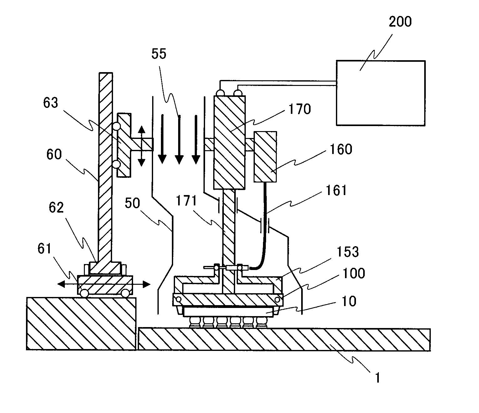
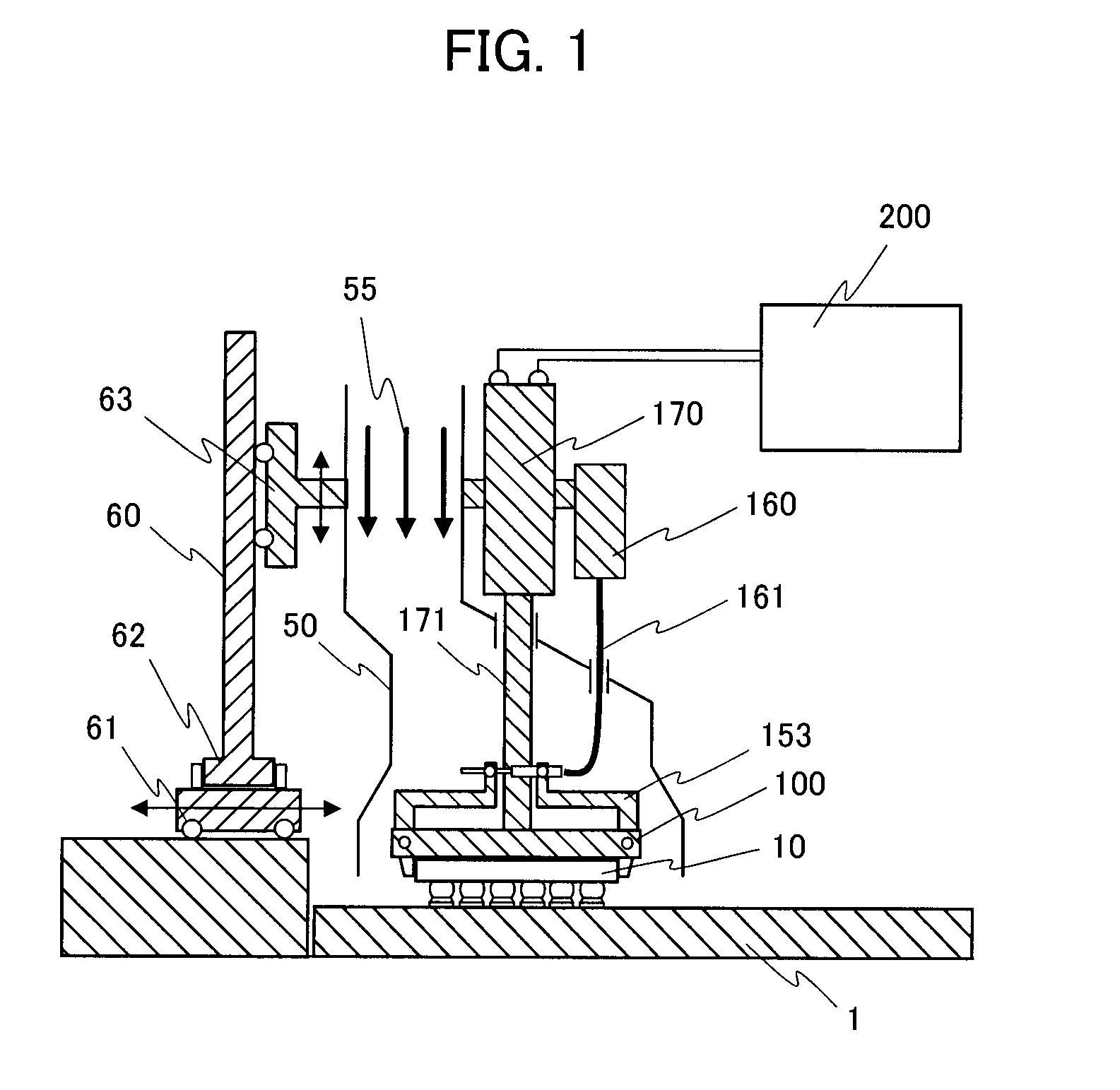
[0057]As a repair apparatus for a miniaturized bump connection component such as a BGA, there was used one that directly applied an output of 100 W of ultrasonic oscillation after the target component was connected to the transducer with the clamp during melting of the solder, and a BGA with full-grid 256 bumps of 1.27 mm-pitch 4-column peripheral arrangement which was poorly connected was removed.

[0058]The BGA was connected by pasting a solder whose composition was the same as that of bumps of an Sn-9Zn solder, so that another BGA which was to be newly exchanged was provided with the bumps of the same Sn-9Zn solder and the BGA was connected again by pasting the Sn-9Zn solder.

[0059]At the time of reconnecting the BGA, the solder bumps and the solder paste were melted 30 seconds later after heating, and 20 seconds later thereafter, cooling of the connection portion by stopping the supply of the hot air and the ultrasonic oscillation for 10 seconds were started. The ultrasonic oscilla...

second embodiment

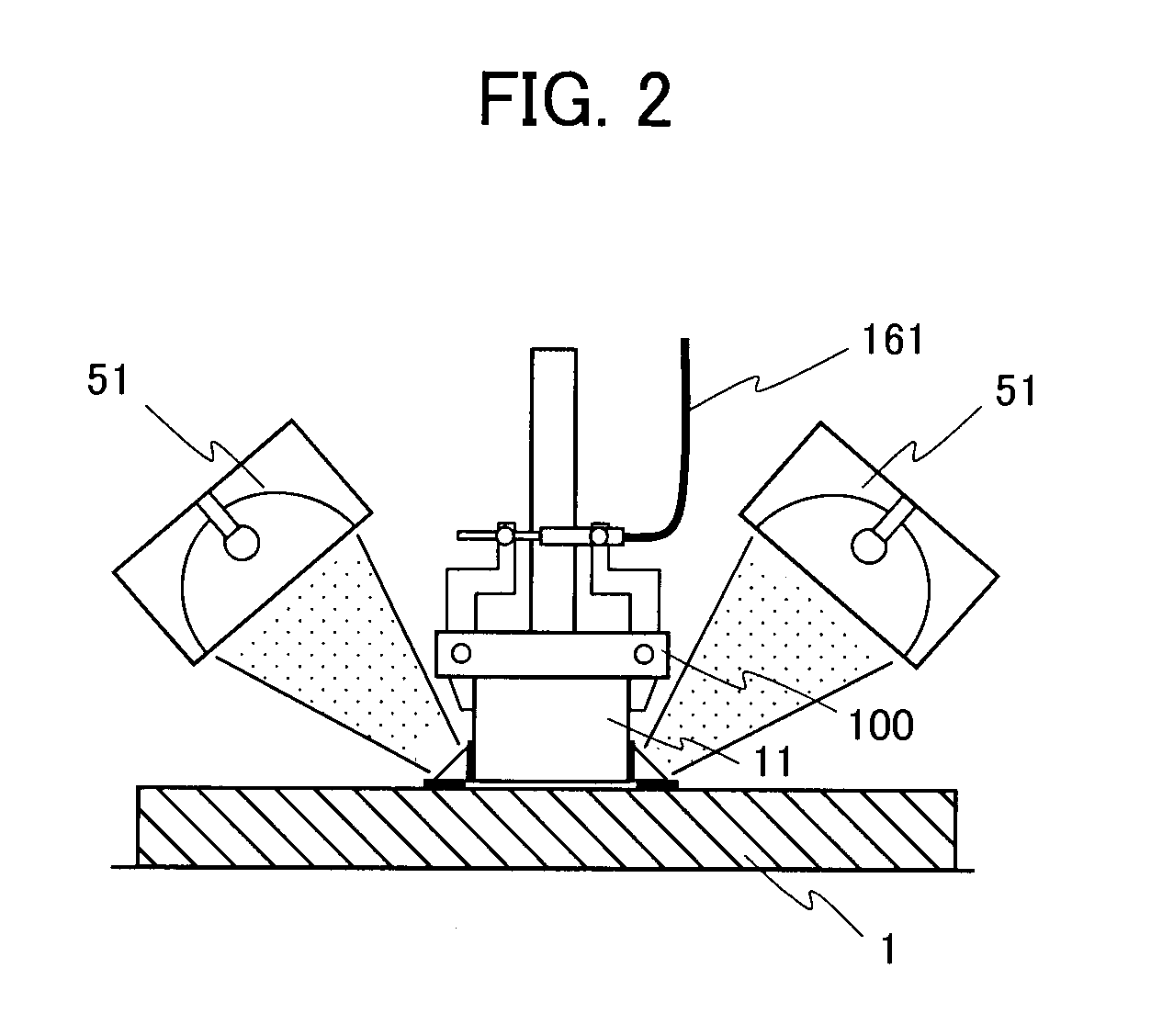
[0065]As a local reflow apparatus for a surface connection component such as a connector, there was used one that directly applied an output of 100 W of ultrasonic oscillation after the electric component was connected to the transducer with the clamp during melting of the solder, and a connector with 0.5 mm-pitch 50-leads was connected to a thin circuit substrate with a thickness of 0.8 mm by pasting an Sn-3Ag-0.5Cu solder.

[0066]At the time of connection, the solder paste was melted 25 seconds later after heating, and 20 seconds later thereafter, cooling of the connection portion by stopping the supply of the hot air and the ultrasonic oscillation for 10 seconds were started.

[0067]The ultrasonic oscillation was applied to the connector with 0.5 mm-pitch 50-leads directly clamped through the transducer of the apparatus.

[0068]Further, the clamp was configured in such a manner that a portion to which the power (power level=about 15N) from the actuator that was provided with the contro...

third embodiment

[0072]As a repair apparatus for a miniaturized bump connection component such as a BGA, there was used one that directly applied an output of 100 W of ultrasonic oscillation after the target component was connected to the transducer with the clamp during melting of the solder, and a BGA with 1.0 mm-pitch full-grid 256 bumps which was poorly connected was removed.

[0073]The BGA was connected by pasting a solder whose composition was the same as that of bumps of an Sn-9Zn solder, so that another BGA which was to be newly mounted was provided with the bumps of the same Sn-9Zn solder and the BGA was connected again by pasting the Sn-9Zn solder.

[0074]At the time of reconnecting the BGA, the solder bumps and the solder paste were melted 30 seconds later after heating, and 20 seconds later thereafter, cooling of the connection portion by stopping the supply of the hot air and the ultrasonic oscillation for up to 20 seconds were started.

[0075]The ultrasonic oscillation was applied to the BGA...


PUM

PropertyMeasurementUnit
oscillation frequencyaaaaaaaaaa
electric poweraaaaaaaaaa
timeaaaaaaaaaa

Abstract

Along with miniaturization of a solder connection portion in a bump repair or a local reflow, a void generated at the time of soldering remains in a solder to remarkably reduce connection strength, and there occurs a non-connection phenomenon in which the solder connection portion and a solder paste are melted, but are not fused with each other. During melting of a solder, a target component is clamped, ultrasonic oscillation is directly applied only to the target component. Further, start of solidification of the solder connection portion is detected by change of an electric impedance of a transducer while applying the ultrasonic oscillation, and the clamp is released before a substrate is warped.

Description

CLAIM OF PRIORITY[0001]The present application claims priority from Japanese Patent Application 2008-180241 filed on Jul. 10, 2008, the content of which is hereby incorporated by reference into this application.BACKGROUND OF THE INVENTION[0002]The present invention relates to a reflow soldering method and a reflow soldering apparatus for realizing the same using a lead-free solder alloy which is low in toxicity but poor in wettability in general. The lead-free solder alloy can be applied to connection of a target component such as an electronic component to a circuit substrate such as an organic substrate, and is an alternative to an Sn-37Pb (unit: % by mass) solder used for soldering at around 220° C.[0003]However, the lead-free solder alloy is generally poor in wettability as compared to the conventional Sn-37Pb solder, and especially in the case of an Sn—Zn solder, wetting of the solder is hardly spread on a connection member. As a result, stress is concentrated at a part where w...

Claims


Application Information

Patent Timeline
Patent Type & Authority Patents(United States)
IPC IPC(8): B23K1/06
CPCB23K1/0016B23K1/0053B23K1/012B23K1/06B23K3/087B23K37/0408B23K37/047H05K3/3436B23K2201/42H05K2203/0285B23K2101/42Y02P70/50
Inventor NAKATSUKA, TETSUYANAKAMURA, MASATO
Owner HITACHI LTD
Learn More