Ohmic contacts to nitrogen polarity GaN

a technology of nitrogen polarity and contact, which is applied in the direction of basic electric elements, electrical equipment, and semiconductor devices, etc., can solve the problems of low contact resistivity on ga-face samples and reduce the height of schottky barriers

Active Publication Date: 2011-09-20
CREELED INC
View PDF71 Cites 58 Cited by
  • Summary
  • Abstract
  • Description
  • Claims
  • Application Information

AI Technical Summary

Problems solved by technology

This reduces the Schottky barrier height to allow for electron tunneling, leading to low contact resistivity on Ga-face samples.

Method used


Image

  • Ohmic contacts to nitrogen polarity GaN
  • Ohmic contacts to nitrogen polarity GaN
  • Ohmic contacts to nitrogen polarity GaN

Examples


Embodiment Construction

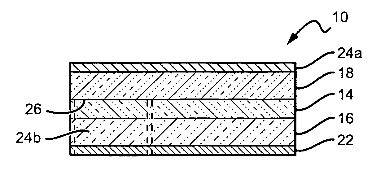
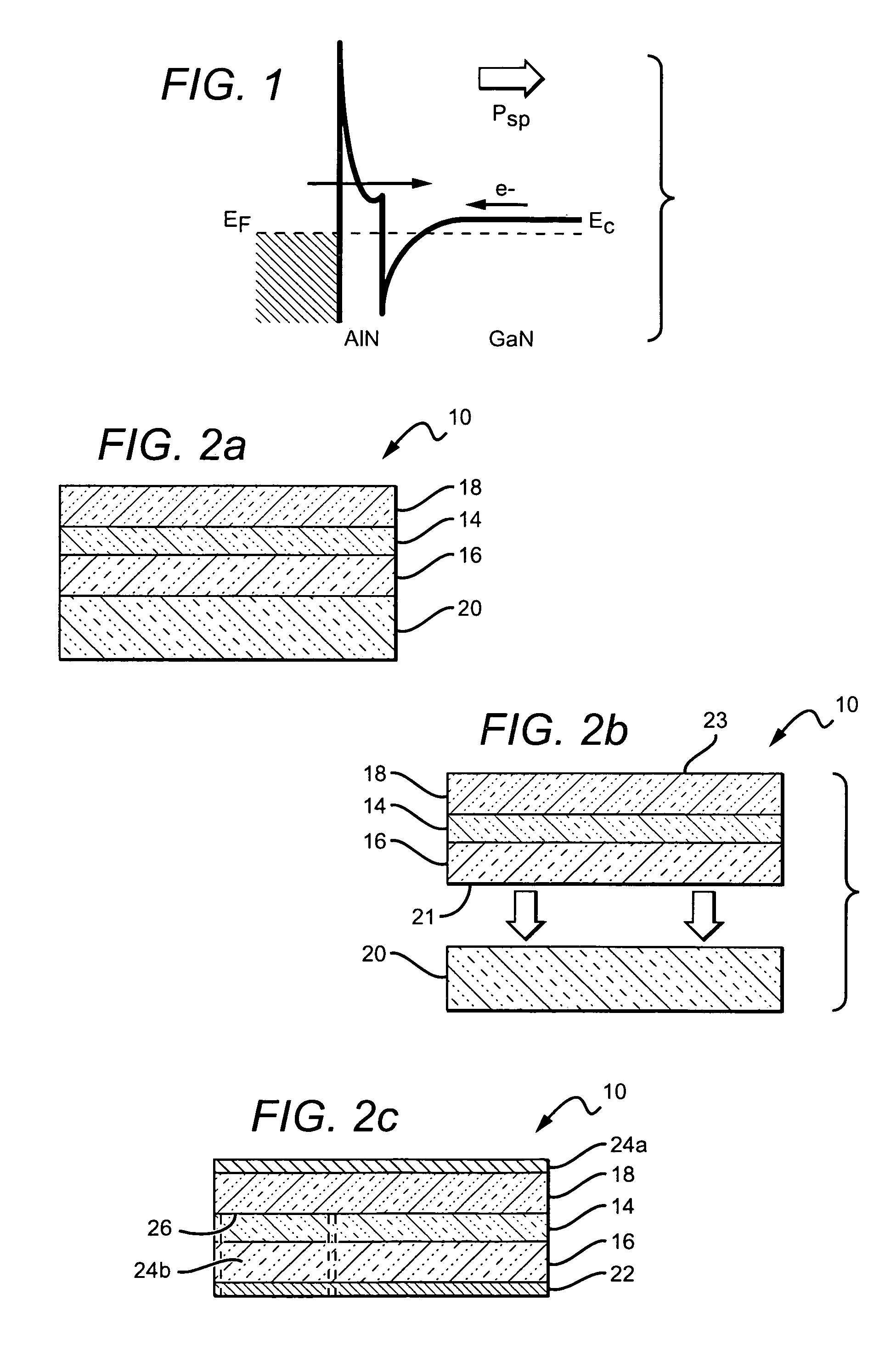
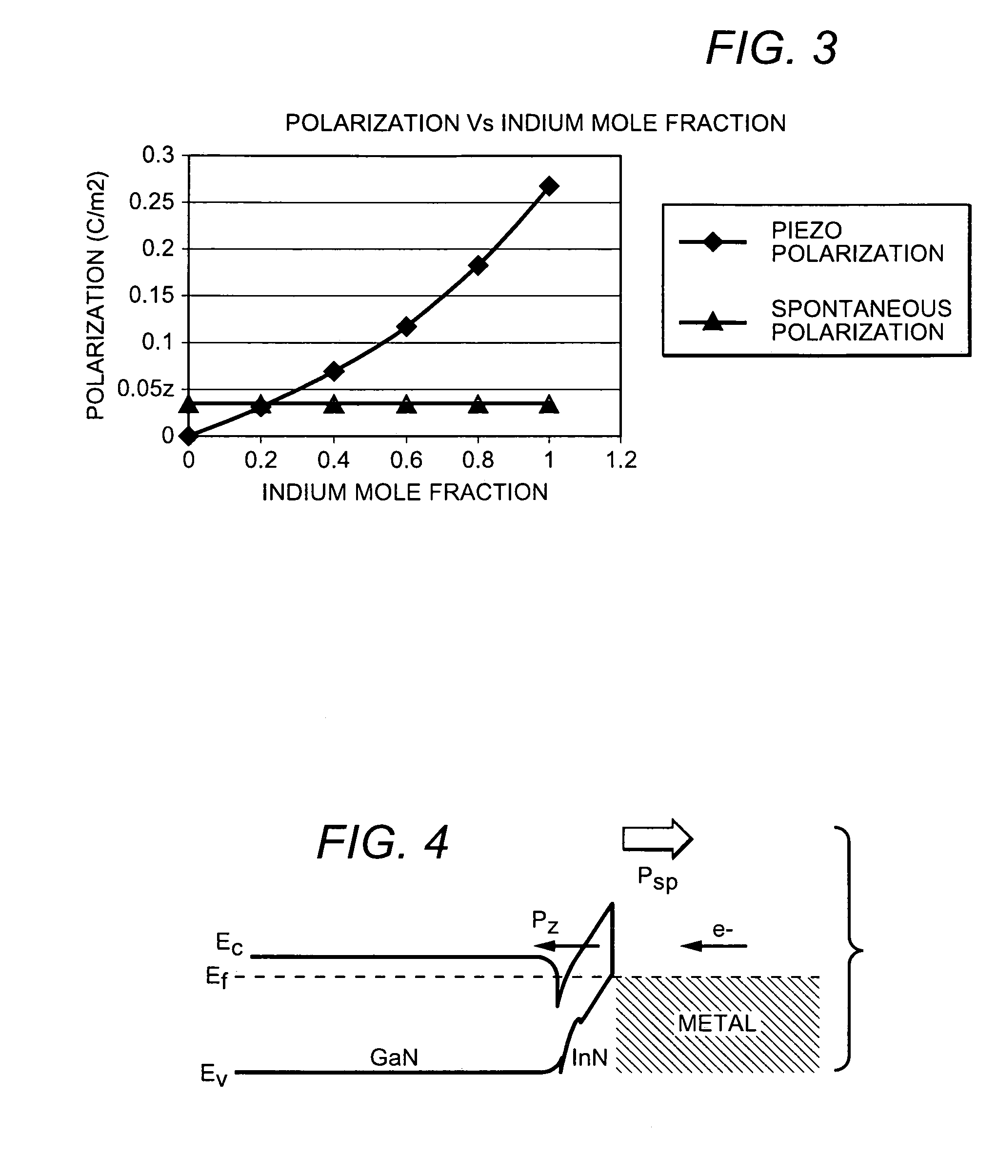
[0022]The present invention is directed to contacting the N-face surface of Group-III nitride epitaxial layers using a material taking advantage of the polarization effects in Group-III nitrides to form ohmic contacts on the N-face. In one embodiment the epitaxial layers comprise the GaN material systems and InN is used as an ohmic contact on the N-face surface of GaN. In other embodiments an embedded InN layer can be included in the epitaxial layers, with conventional contact materials then used for forming the ohmic contact to the N-face.

[0023]The present invention is described herein with reference to certain embodiments but it is understood that the invention can be embodied in many different forms and should not be construed as limited to the embodiments set forth herein. In particular, the present invention is described below in regards to Group-III nitride LEDs, but can also be applied to contacting other devices, including but not limited to solid state lasers.

[0024]It is al...


PUM

PropertyMeasurementUnit
thicknessesaaaaaaaaaa
face polaritiesaaaaaaaaaa
polarityaaaaaaaaaa

Abstract

Contacting materials and methods for forming ohmic contact to the N-face polarity surfaces of Group-III nitride based semiconductor materials, and devices fabricated using the methods. One embodiment of a light emitting diode (LED) a Group-III nitride active epitaxial region between two Group-III nitride oppositely doped epitaxial layers. The oppositely doped layers have alternating face polarities from the Group III and nitrogen (N) materials, and at least one of the oppositely doped layers has an exposed surface with an N-face polarity. A first contact layer is included on and forms an ohmic contact with the exposed N-face polarity surface. In one embodiment, the first contact layer comprises indium nitride.

Description

[0001]The application claims the benefit of U.S. provisional patent application Ser. No. 60 / 899,247 to Ashay Chitnis, filed on Feb. 1, 2007.BACKGROUND OF THE INVENTION[0002]1. Field of the Invention[0003]This invention relates to light emitting diodes, and in particular to forming ohmic contacts on the nitrogen face polarity surfaces of gallium nitride based light emitting diodes.[0004]2. Description of the Related Art[0005]Light emitting diodes (LED or LEDs) are solid state devices that convert electric energy to light, and generally comprise one or more active layers of semiconductor material sandwiched between oppositely doped n-type and p-type layers. When a bias is applied across the doped layers, holes and electrons are injected into the active layer where they recombine to generate light. Light is emitted from the active layer and from all surfaces of the LED.[0006]For typical LEDs it is desirable to operate at the highest light emission efficiency, and one way emission effic...

Claims


Application Information

Patent Timeline
Patent Type & Authority Patents(United States)
IPC IPC(8): H01L21/00H01L27/15H01L29/165H01L33/00H01L31/153H01L31/12H01L33/32H01L33/40
CPCH01L33/0079H01L33/32H01L33/40H01L33/0093
Inventor CHITNIS, ASHAY
Owner CREELED INC
Why Eureka
Try Eureka