
Semiconductor device manufacturing method and semiconductor manufacturing apparatus

a semiconductor and manufacturing method technology, applied in the direction of chemistry apparatus and processes, cleaning using liquids, coatings, etc., can solve the problems of occurrence of wiring shorts, deterioration of withstand voltage between elements, etc., to achieve reliably hydrogen termination, shorten the treatment time of hf2 ions, and increase the speed of hydrogen termination

Inactive Publication Date: 2011-10-04
OHMI TADAHIRO
View PDF18 Cites 0 Cited by
  • Summary
  • Abstract
  • Description
  • Claims
  • Application Information

AI Technical Summary

Benefits of technology

"The invention aims to provide a more efficient method for hydrogen termination of silicon surfaces by adding an oxidant to a solution containing dilute hydrofluoric acid. The speed of hydrogen termination is increased by adding an oxidant. The invention also provides a method and apparatus for manufacturing an electrically reliable semiconductor device by realizing the hydrogen termination. The contact angle of pure water on a Si surface is measured and found to be the main factor in determining the surface's hydrophobicity. The Si (110) surface is found to have difficulty in realizing hydrophobicity as compared to the Si (100) surface. The Si (110) surface is easily terminated with Si—OH bonds, while the Si (110) surface is easily terminated with Si—F bonds. The Si—OH bonds formed on the Si surface are stable and can lead to the formation of Si—H bonds. The surface orientation also affects the hydrogen termination speed, with certain surfaces having slow hydrogen termination speeds."

Problems solved by technology

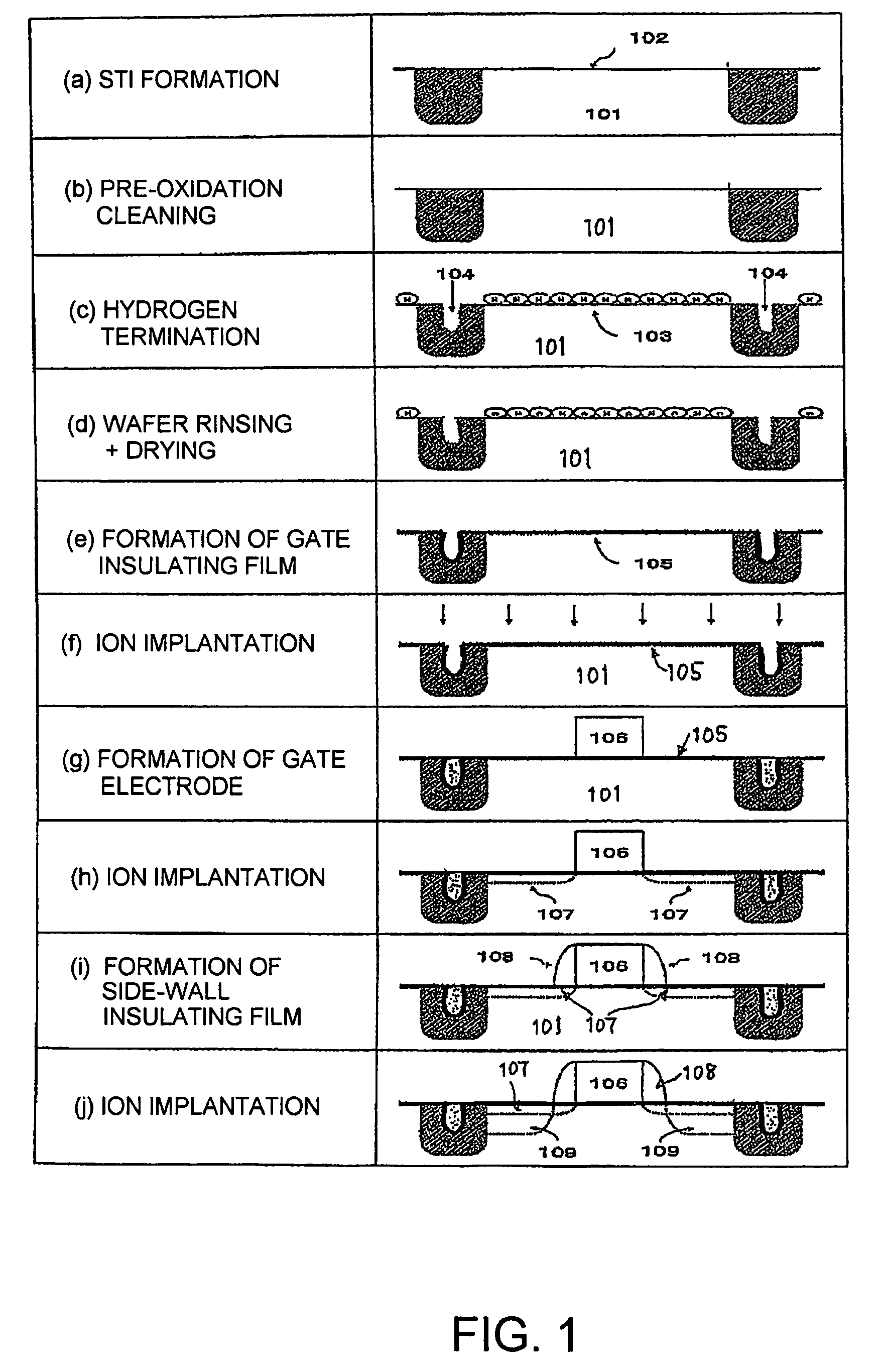
When the integrated circuit is completed, this polycrystalline silicon embedded in the void 104 causes deterioration of withstand voltage between the elements and further causes occurrence of wiring shorts.
By the treatment for about 10 minutes, etching of an STI silicon oxide film proceeds like in the case of FIG. 1, thus causing deterioration of withstand voltage between elements and wiring shorts.

Method used


Image

  • Semiconductor device manufacturing method and semiconductor manufacturing apparatus
  • Semiconductor device manufacturing method and semiconductor manufacturing apparatus
  • Semiconductor device manufacturing method and semiconductor manufacturing apparatus

Examples


embodiment 1

[0063]As the first embodiment, manufacturing processes of a field-effect transistor constituting an integrated circuit formed in a semiconductor region will be described using an LDD (Lightly Doped Drain)-structure n-type field-effect transistor as an example. FIG. 10 shows the transistor flow.

[0064]Element isolation is carried out, for example, by an STI (Shallow Trench Isolation) method, thereby forming an element region 1002 including source, drain, and channel regions on the surface of a p-type (110) silicon wafer 1001 (FIG. 10(a)). Pre-oxidation cleaning such as RCA cleaning is applied to the element region 1002 (FIG. 10(b)) to remove organic compounds, particles, and metal impurities and, thereafter, treatment is carried out using a solution in which H2O2 is added in an amount of 0.5 wt % to 0.5 wt % hydrofluoric acid. The etching time in this event is 1 minute. Subsequently, rinsing with pure water is performed to hydrogen-terminate 1003 the element region 1002 (FIG. 10(c)).

[...

embodiment 2

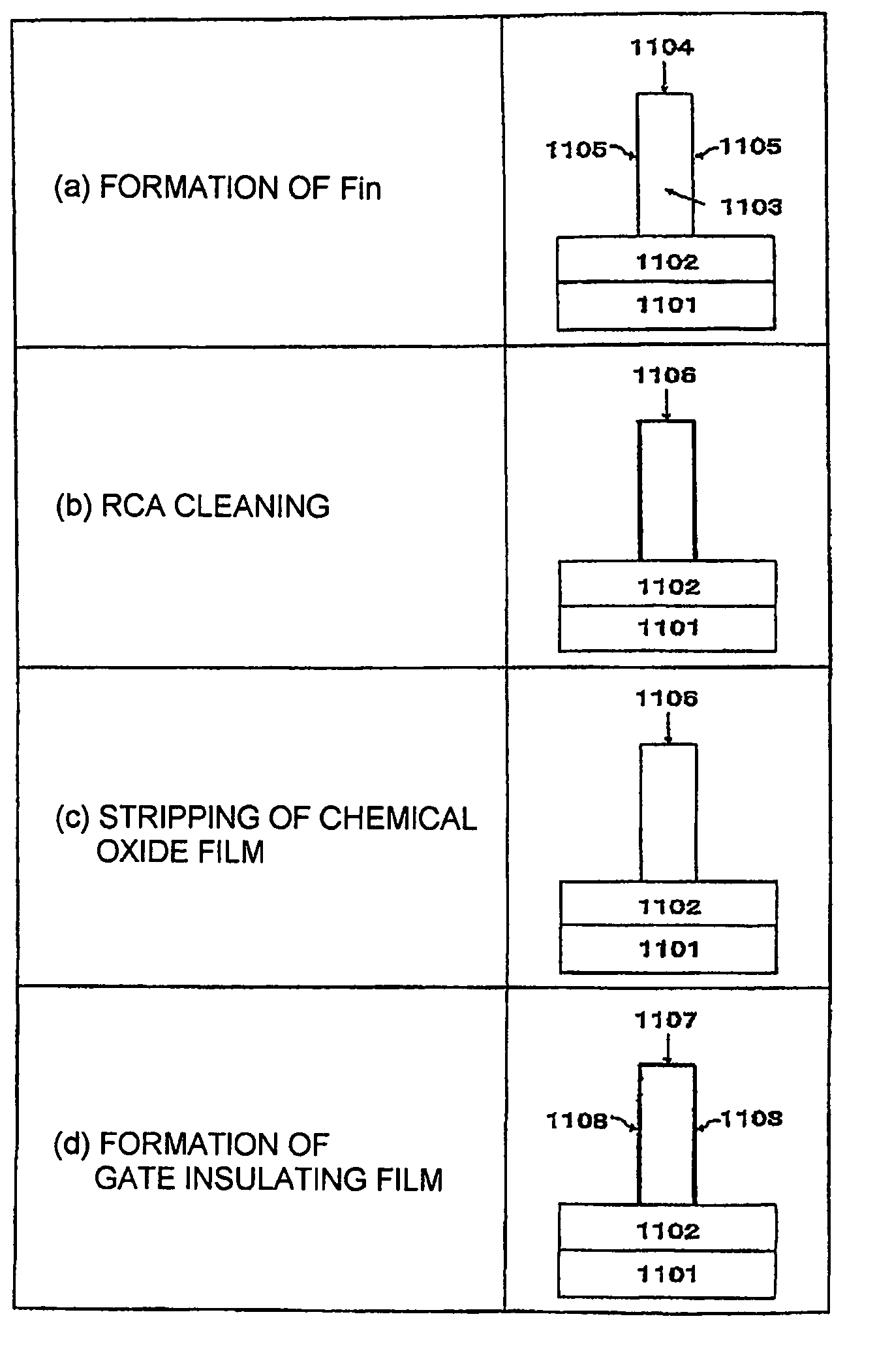
[0081]Next, as the second embodiment, there are shown states before and after formation of a gate insulating film of a Fin-FET.

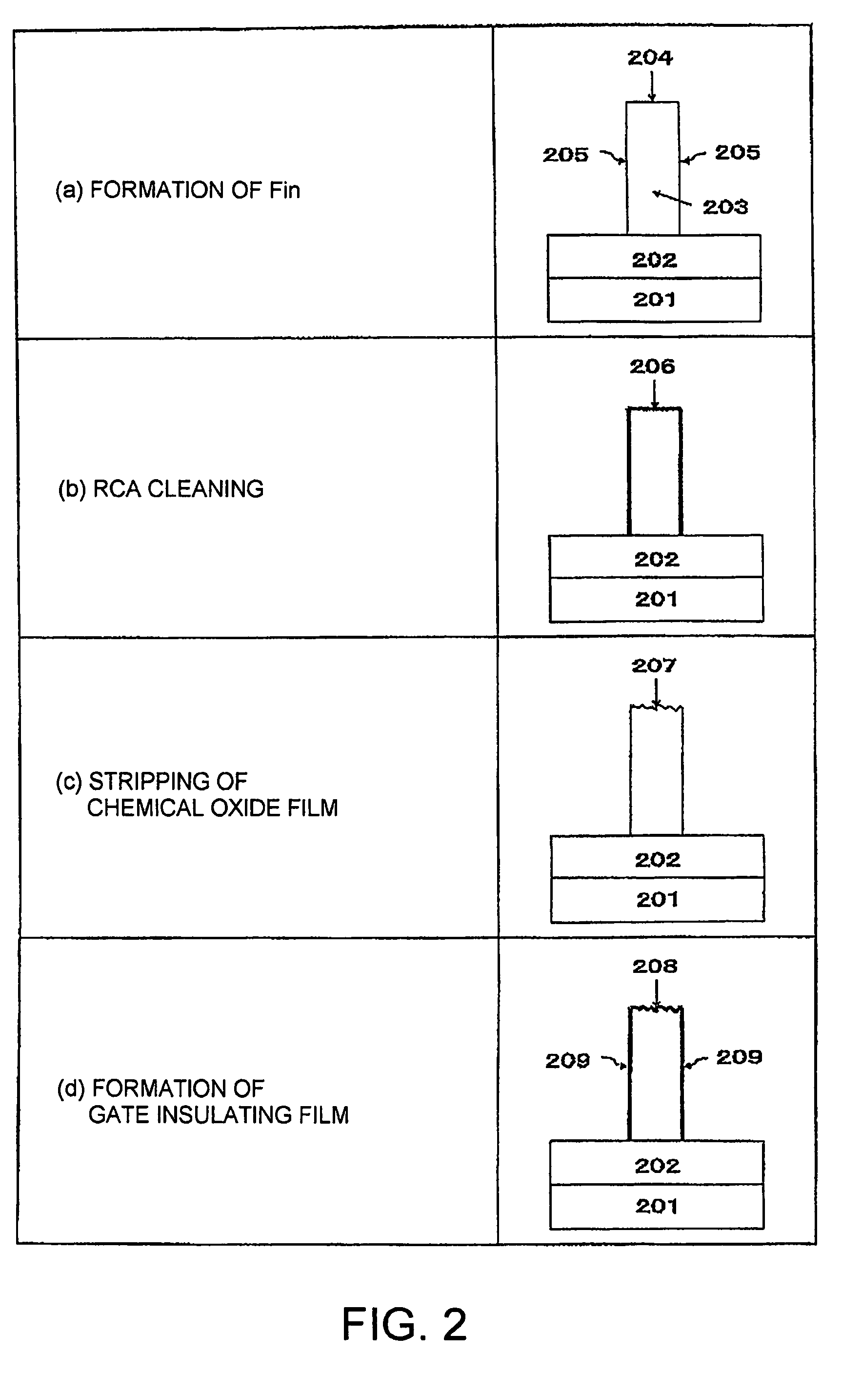
[0082]FIG. 11(a) is a section of an element region as seen in a direction from source to drain. Si02 1102 is formed on a Si substrate 1101 and a Fin 1103 is formed thereon. The element region comprises a Si (100) surface 1104 and Si (110) surfaces 1105. After performing acid cleaning (HCI / H2O2 cleaning) in RCA cleaning, a chemical oxide film 1106 is formed (FIG. 11(b)). Thereafter, treatment is carried out using a solution in which 0.5 wt % H2O2 is added to 0.5 wt % dilute hydrofluoric acid, thereby stripping the chemical oxide film 1106. The stripping time is 1 minute. Using this solution, the chemical oxide film 1106 is stripped in about 30 seconds regardless of the surface orientation and, thereafter, hydrogen termination is achieved with overetching for about 30 seconds. Owing to the short-time etching for about 1 minute, etching of an STI silicon oxide ...


PUM

PropertyMeasurementUnit
contact angleaaaaaaaaaa
thicknessaaaaaaaaaa
termination speedaaaaaaaaaa

Abstract

By hydrogen-terminating a semiconductor surface using a solution containing HF2− ions and an oxidant, the hydrogen termination can be quickly carried out. In this case, the semiconductor surface is silicon having a (111) surface, a (110) surface, or a (551) surface.

Description

[0001]This application is the National Phase of PCT / JP2005 / 017260, filed Sep. 20, 2005, the disclosure of which is hereby incorporated by reference in its entirety.TECHNICAL FIELD[0002]This invention relates to a method of quickly carrying out hydrogen termination treatment of a semiconductor surface and further relates to an apparatus for carrying out such hydrogen termination treatment and a product such as a semiconductor device obtained by carrying out such hydrogen termination treatment.BACKGROUND ART[0003]Manufacturing processes of a field-effect transistor constituting an integrated circuit formed in a semiconductor region will be described with reference to FIG. 1, using an LDD (Lightly Doped Drain)-structure n-type field-effect transistor as an example.[0004]At first, element isolation is carried out, for example, by an STI (Shallow Trench Isolation) method, thereby forming an element region 102 on the surface of a p-type (110) surface silicon 101 serving as a semiconductor...

Claims


Application Information

Patent Timeline
Patent Type & Authority Patents(United States)
IPC IPC(8): H01L21/461B08B7/04
CPCH01L21/306H01L29/045H01L29/6659H01L29/66795H01L29/785H01L21/304
Inventor OHMITERAMOTO, AKINOBUAKAHORI, HIROSHI
Owner OHMI TADAHIRO
Learn More