Substrate structrue for light-emitting diode

a technology of light-emitting diodes and substrate structures, which is applied in the direction of semiconductor devices, printed circuit aspects, solid-state devices, etc., can solve the problems of increased manufacturing costs, increased flaw rate of products, and large size, so as to reduce costs, enhance the passing rate of manufactured products, and eliminate potential flaws of failure soldering.

Inactive Publication Date: 2011-10-04
HAYASHIBARA BIOCHEMICAL LAB INC
View PDF3 Cites 70 Cited by
  • Summary
  • Abstract
  • Description
  • Claims
  • Application Information

AI Technical Summary

Benefits of technology

[0005]An objective of the present invention is to provide a substrate structure for light-emitting diode (LED) featuring a combination of an upper layer substrate, a flexile printed circuit, a lower layer substrate, and an isolation substance, which requires no surface mount technology neither adhesive application and solder application and solder oven process are needed for soldering a substrate and a flexible printed circuit together, thereby eliminating the potential flaw of failure soldering between the substrate and the flexible printed circuit, enhancing the passing rate of the manufactured products and reducing the costs for enhancing practicability and convenience.
[0006]Another objective of the present invention is to provide a substrate structure for LED, featuring a combination of an upper layer substrate, a flexile printed circuit, a lower layer substrate, and an isolation substance, wherein laminating the flexible printed board between the upper layer substrate and the lower layer substrate effectively eliminates the weak points occurring at the soldered portions between the flexible printed board and the substrate to allow for flexed arrangement of the device and breaking through the constraints imposed by a limited installation space, making more flexible use and application, thereby enhancing practicability and convenience.
[0007]Another objective of the present invention is to provide a substrate structure for LED, featuring a combination of an upper layer substrate, a flexile printed circuit, a lower layer substrate, and an isolation substance, wherein the laminated structure effectively makes the circuit board compact and, when applied to a light-emitting chip, can substantially reduce the overall size of the light-emitting diode (LED) to be suitable for light-emitting strips of different lengths and miniaturized electronic devices to thereby enhance the practicability and convenience.
[0008]A further objective of the present invention is to provide a substrate structure for LED, featuring a combination of an upper layer substrate, a flexile printed circuit, a lower layer substrate, and an isolation substance, wherein interposing the flexible printed board between the upper and lower substrates provides enhanced resistance against bending, flexing, and stretching that might occur in general application of the product, so as to enhance the overall practicability and convenience.
[0009]To realize the above objectives, in accordance with the present invention, a substrate structure for light-emitting diode (LED) is provided, comprising an upper layer substrate, a flexible printed circuit, a lower layer substrate, and an isolation substance. The upper layer substrate has forming a conductor pattern to provide a bonding zone and a plurality of electrode zones. The flexible printed circuit is bonded under the upper layer substrate. The lower layer substrate is bonded under the flexible printed circuit and has forming conductor lines. The isolation substance is coated on the top surface of the upper layer substrate and the bottom surface of the lower layer substrate. As such, a substrate structure comprised of upper and lower layers made of the upper-layer and lower-layer substrates interposing a core made of the flexible printed circuit is formed, which enhances practicability and convenience.

Problems solved by technology

However, the conventional LEDs, no matter how small the size of a carrier thereof is, are of a bulky size after a light-transmitting layer is wrapped around the constituent components thereof.
This is susceptible to potential risks of failure soldering between the insulation substrate B and the flexible printed circuit A, leading to increased flaw rate of products and also increasing manufacturing costs.
When the flexible printed circuit A and the insulation substrate B are fixed together by soldering, the insulation substrate B occupies a substantial amount of the surface area, leading to increase of surface area of a unit volume, and for applications in a bent or flexed condition, the soldered portions between the flexible printed circuit A and the insulation substrate B become weak points in view of structural strength, leading to undesired separation of the flexible printed circuit A from the insulation substrate B and consequently poor electrical engagement therebetween.
Further, the conventional structure is commonly used in an application for a light-emitting strip, wherein up-and-down bending, flexing and stretching occur very often, and the soldered structure of the insulation substrate B soldered to the flexible printed circuit is structurally poor in resisting flexing and stretching.

Method used


Image

  • Substrate structrue for light-emitting diode
  • Substrate structrue for light-emitting diode
  • Substrate structrue for light-emitting diode

Examples


Embodiment Construction

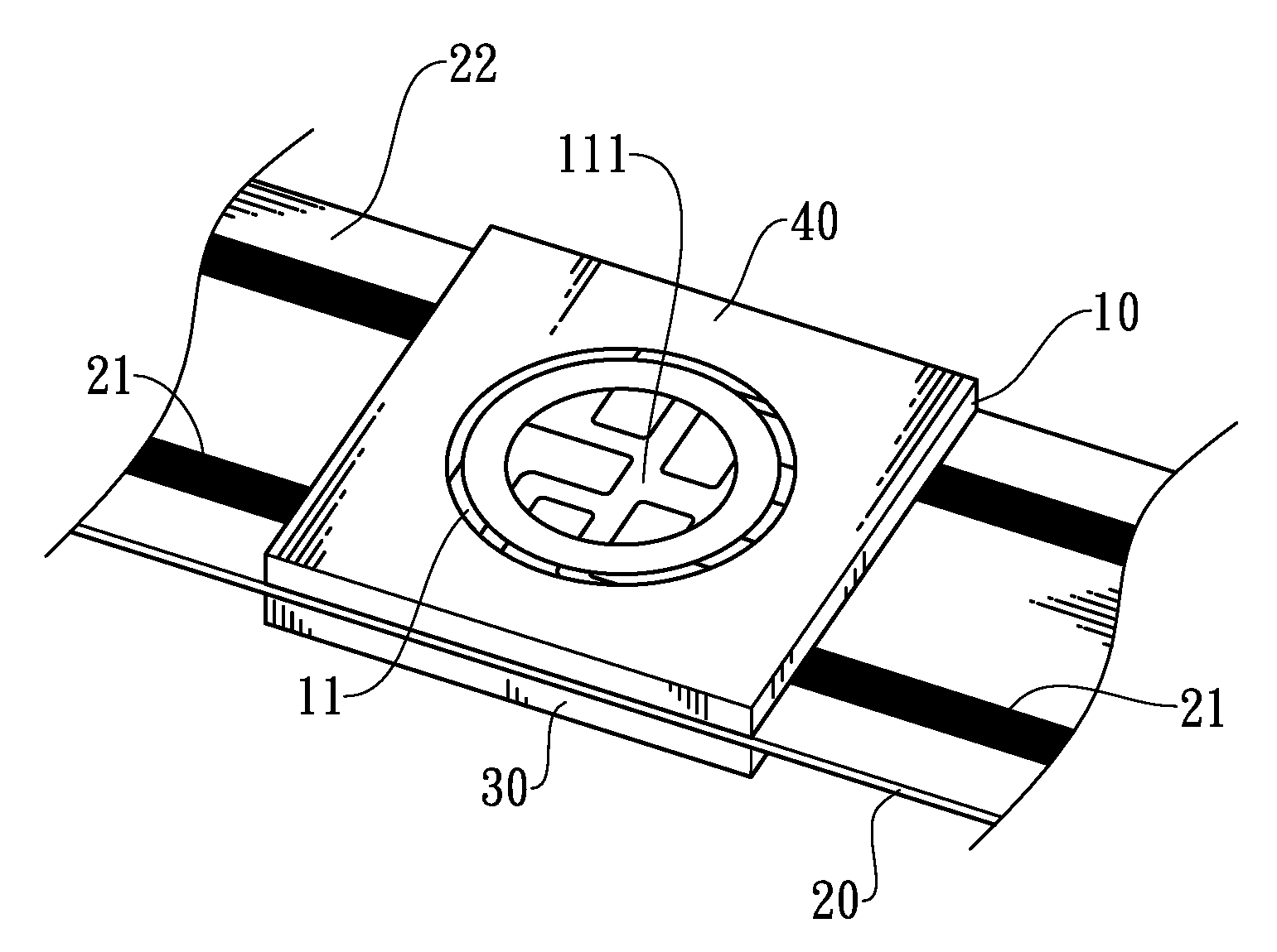
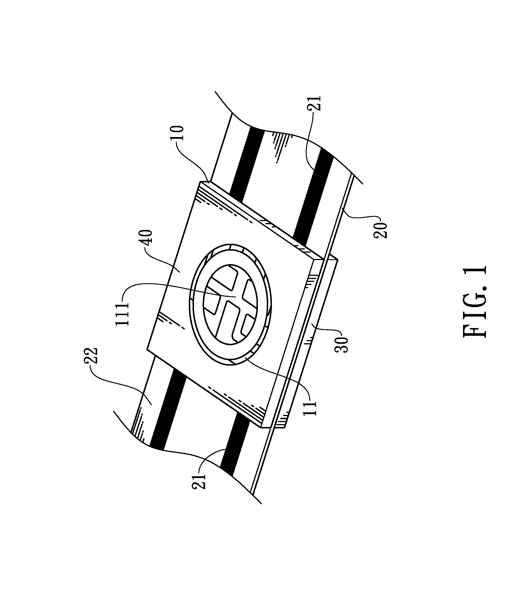
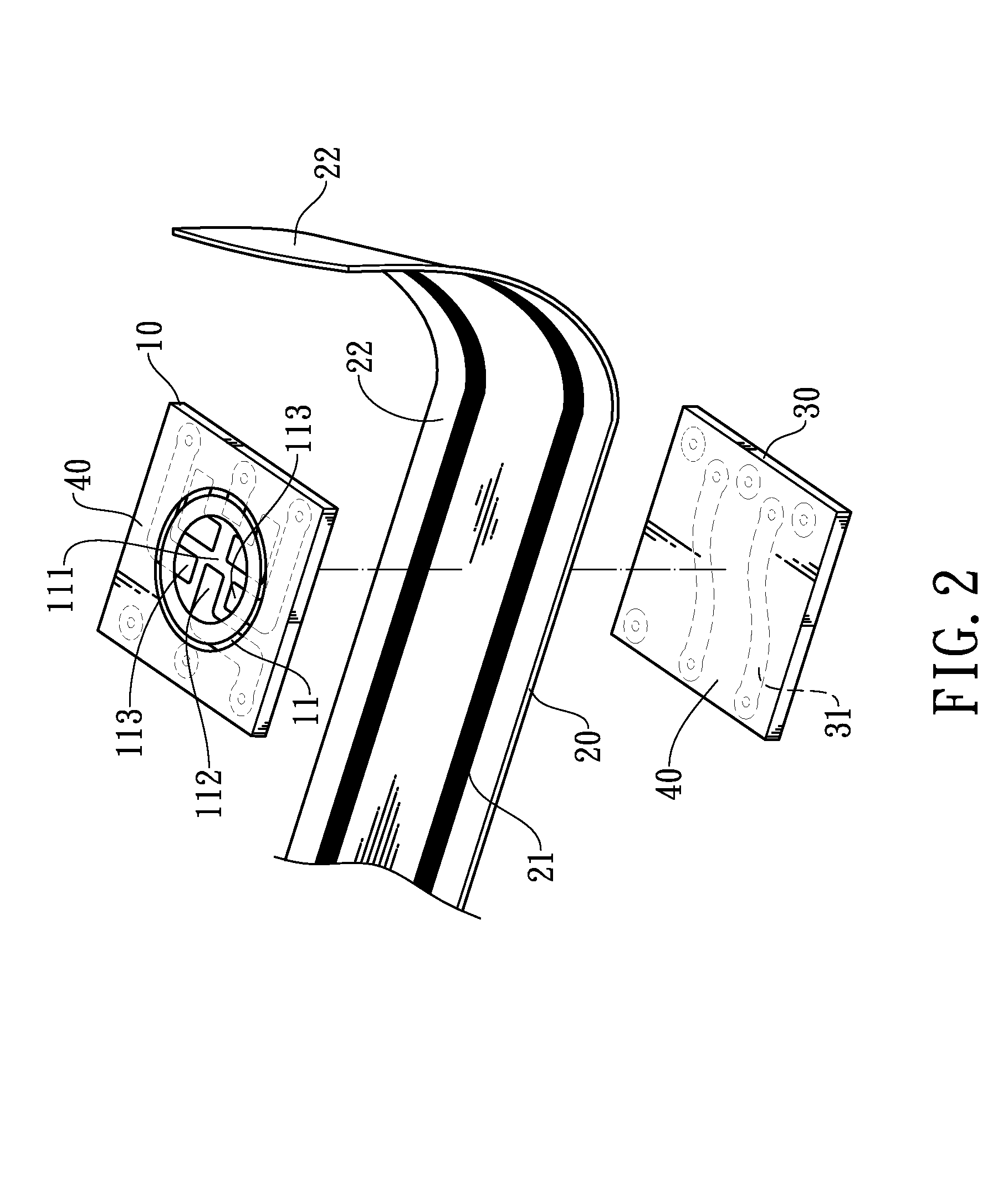
[0017]With reference to the drawings and in particular to FIGS. 1-4, which show a substrate structure for a light-emitting diode (LED) constructed in accordance with the present invention, the substrate structure of the present invention comprises an upper layer substrate 10, which comprises an insulation substrate, which can be for example a printed circuit board (PCB), a glass fiber board (such as FR-4), a temperature-resistant glass fiber board (such as FR5), a ceramic substrate, a metal-core PCB (MCPCB), a direct copper bonded (DCB) substrate, a metal composite board, a copper-coated aluminum board, or an aluminum board. The upper layer substrate 10 has a top face on which a conductor pattern 11 is formed. The conductor layer 11 is formed by coating a conductor layer on the top surface of the upper-layer substrate 10, followed by etching to form a desired layout of conductor lines. The conductor layer 11 is formed to comprise a bonding zone 111 and a plurality of electrode zones...


PUM


Abstract

Disclosed is a substrate structure for light-emitting diode (LED), including an upper layer substrate, a flexible printed circuit, a lower layer substrate, and an isolation substance. The upper layer substrate has forming a conductor pattern to provide a bonding zone and a plurality of electrode zones. The flexible printed circuit is bonded under the upper layer substrate. The lower layer substrate is bonded under the flexible printed circuit and has forming conductor lines. The isolation substance is coated on the top surface of the upper layer substrate and the bottom surface of the lower layer substrate. As such, a substrate structure comprised of upper and lower layers made of the upper-layer and lower-layer substrates interposing a core made of the flexible printed circuit is formed.

Description

FIELD OF THE INVENTION[0001]The present invention relates to a substrate structure for light-emitting diode (LED), and in particular to a substrate structure featuring a combination of an upper layer substrate, a flexile printed circuit, a lower layer substrate, and an isolation substance, which is formed by laminating the flexible printed circuit between the upper layer substrate and the lower layer substrate so that no surface mount technology, neither adhesive application and solder application and solder oven process, is needed, thereby eliminating the potential flaw of failure soldering between the substrate and the flexible printed circuit, enhancing the passing rate of the manufactured products and reducing the costs for being applicable to the substrate for light-emitting chips.BACKGROUND OF THE INVENTION[0002]Light-emitting diodes (LEDs) are of the advantages of low power consumption and long lifespan and are thus commonly used in electronic products. With the progress of s...

Claims


Application Information

Patent Timeline
Patent Type & Authority Patents(United States)
IPC IPC(8): H01L33/00
CPCH05K1/189H01L33/641H05K2201/10106H01L2224/48091H01L2924/00014
Inventor LIN, YUAN
Owner HAYASHIBARA BIOCHEMICAL LAB INC
Why Eureka
Try Eureka