Multilayer film structure for increasing transmittance and method for manufacturing the same

a multi-layer film and transmittance technology, applied in the direction of instruments, natural mineral layered products, transportation and packaging, etc., can solve the problems of difficult to conform to the required spectrogram, bad chromatic characteristics of the pdp filter, etc., to achieve high volume production, increase transmittance, and high reliability

Inactive Publication Date: 2011-10-11
INNOVATION & INFINITY GLOBAL
View PDF3 Cites 0 Cited by
  • Summary
  • Abstract
  • Description
  • Claims
  • Application Information

AI Technical Summary

Benefits of technology

[0009]One particular aspect of the present invention is to provide a multilayer film structure for increasing transmittance. The process of manufacturing the multilayer film structure in high volume production is highly reliable and has been routinely used in industries such as semiconductor manufacturing, disc head manufacturing, LCD manufacturing, CRT manufacturing, architecture glass manufacturing, touch sensor display manufacturing, screen filter manufacturing and plastic web for more than twenty years.

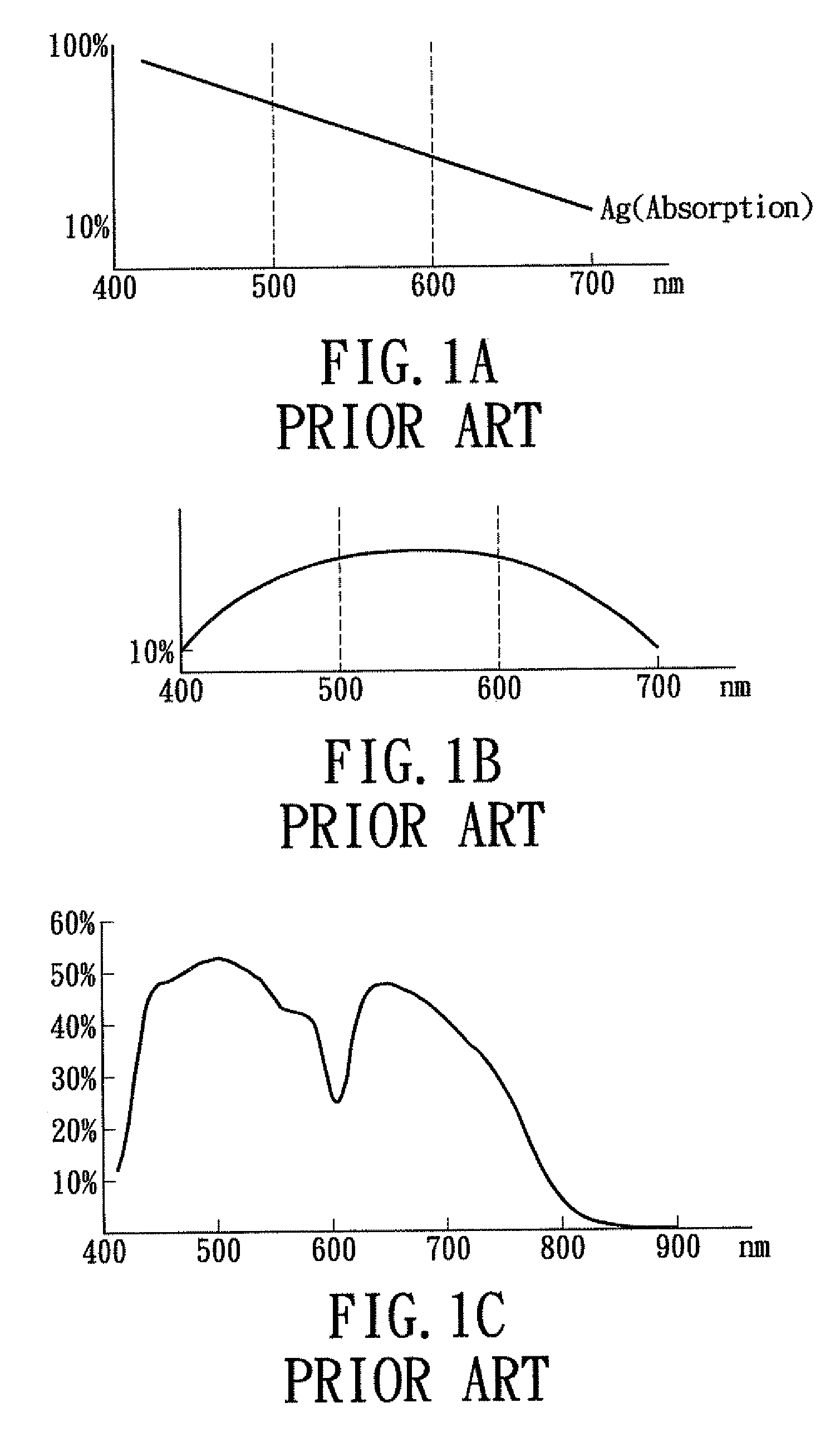
Problems solved by technology

Hence, it is difficult to conform to the required spectrogram, and the chromatic characteristics of the PDP filter are bad.

Method used


Image

  • Multilayer film structure for increasing transmittance and method for manufacturing the same
  • Multilayer film structure for increasing transmittance and method for manufacturing the same
  • Multilayer film structure for increasing transmittance and method for manufacturing the same

Examples


first embodiment

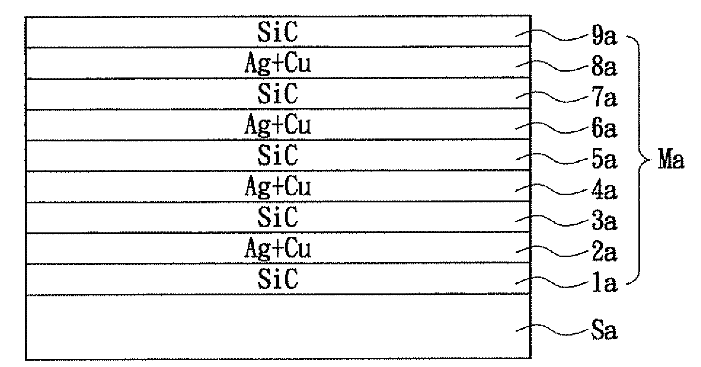
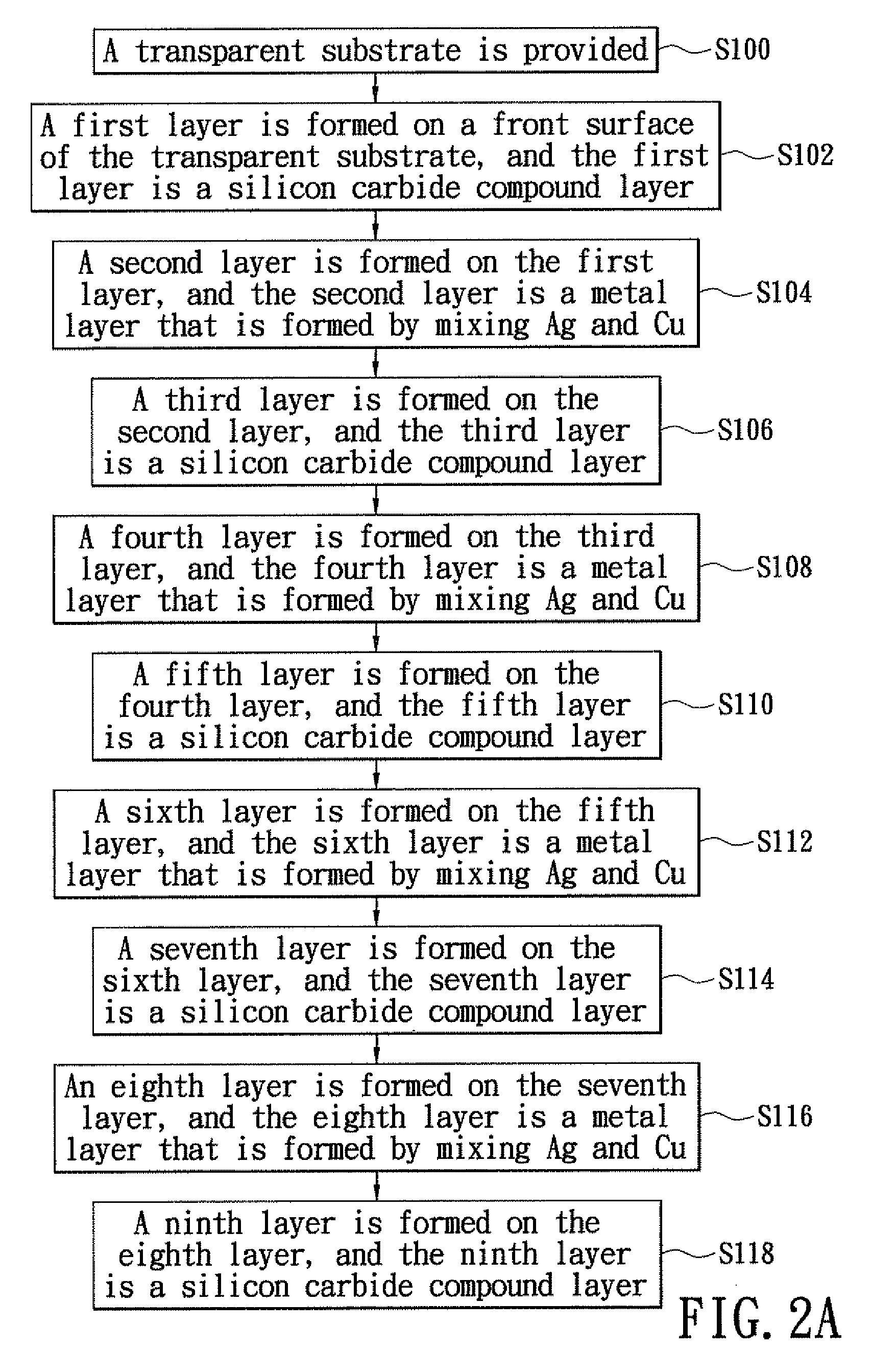
[0035]Referring to FIG. 2A, the present invention provides a method for manufacturing a multilayer film structure for increasing transmittance. The method includes:

[0036]S100: a transparent substrate Sa is provided;

[0037]S102: a first layer 1a is formed on a front surface of the transparent substrate Sa, and the first layer 1a is a silicon carbide compound layer (dielectric layer);

[0038]S104: a second layer 2a is formed on the first layer 1a, and the second layer 2a is a metal layer that is formed by mixing Ag and Cu;

[0039]S106: a third layer 3a is formed on the second layer 2a, and the third layer 3a is a silicon carbide compound layer;

[0040]S108: a fourth layer 4a is formed on the third layer 3a, and the fourth layer 4a is a metal layer that is formed by mixing Ag and Cu;

[0041]S110: a fifth layer 5a is formed on the fourth layer 4a, and the fifth layer 5a is a silicon carbide compound layer;

[0042]S112: a sixth layer 6a is formed on the fifth layer 5a, and the sixth layer 6a is a m...

second embodiment

[0055]Referring to FIGS. 3A and 3B, the present invention provides a method for manufacturing a multilayer film structure for increasing transmittance. The method includes:

[0056]S200: a transparent substrate Sb is provided;

[0057]S202: a first layer 1b is formed on a front surface of the transparent substrate Sb, and the first layer 1b is a mixed layer (dielectric layer) that is composed of silicon carbide compound and Ti-based oxide;

[0058]S204: a second layer 2b is formed on the first layer 1b, and the second layer 2b is a metal layer that is formed by mixing Ag and Cu;

[0059]S206: a third layer 3b is formed on the second layer 2b, and the third layer 3b is a mixed layer that is composed of silicon carbide compound and Ti-based oxide;

[0060]S208: a fourth layer 4b is formed on the third layer 3b, and the fourth layer 4b is a metal layer that is formed by mixing Ag and Cu;

[0061]S210: a fifth layer 5b is formed on the fourth layer 4b, and the fifth layer 5b is a mixed layer that is comp...

third embodiment

[0068]Referring to FIGS. 4A and 4B, the present invention provides a method for manufacturing a multilayer film structure for increasing transmittance. The method includes:

[0069]S300; a transparent substrate Sc is provided;

[0070]S302: a first layer 1c is formed on a front surface of the transparent substrate Sc, and the first layer 1c is a Ti-based oxide layer (dielectric layer);

[0071]S304: a second layer 2c is formed on the first layer 1c, and the second layer 2c is a metal layer that is formed by mixing Ag and Cu;

[0072]S306: a third layer 3c is formed on the second layer 2c, and the third layer 3c is a Ti-based oxide layer;

[0073]S308: a fourth layer 4c is formed on the third layer 3c, and the fourth layer 4c is a metal layer that is formed by mixing Ag and Cu;

[0074]S310: a fifth layer 5c is formed on the fourth layer 4c, and the fifth layer 5c is a Ti-based oxide layer;

[0075]S312: a sixth layer 6c is formed on the fifth layer 5c, and the sixth layer 6c is a metal layer that is for...


PUM

PropertyMeasurementUnit
transmittanceaaaaaaaaaa
thicknessaaaaaaaaaa
thicknessaaaaaaaaaa

Abstract

A multilayer film structure for increasing transmittance includes a transparent substrate and a multifunctional film module. The multifunctional film module is formed on a front surface of the transparent substrate and composed of a plurality of dielectric layers and a plurality of metal layers. The dielectric layers and the metal layers are alternately stacked onto each other, and each metal layer is formed by mixing at least two metals. Each dielectric layer is a silicon carbide compound layer that is SiC, and each metal layer is formed by mixing Ag and Cu.

Description

BACKGROUND OF THE INVENTION[0001]1. Field of the Invention[0002]The present invention relates to a structure and a method for manufacture the same, and particularly relates to a multilayer film structure for increasing transmittance and a method for manufacturing the same.[0003]2. Description of Related Art[0004]In the prior art, the method for manufacturing a plasma display panel (PDP) filter comprises two steps. The first step is a sputtering process that includes forming a multifunctional film module on a transparent glass in order to generate functions such as anti-EMI, anti-reflection and near infrared ray absorption. The second step is: manufacturing a film with a coated dye to control color in order to conform to the required spectrogram, and then attaching the film with the coated dye onto the multifunctional film module of the transparent glass. The manufacturing of the PDP filter is accomplished by said two steps.[0005]However, the spectrogram plot of the multifunctional f...

Claims


Application Information

Patent Timeline
Patent Type & Authority Patents(United States)
IPC IPC(8): B32B7/00B32B15/00B05D1/36B05D5/00
CPCG02B1/115Y10T428/24975Y10T428/1045Y10T428/265C09K2323/033Y10T428/31678
Inventor CHANG, CHENG-CHIEHLIU, HSIU-FENGKUO, PI-JUI
Owner INNOVATION & INFINITY GLOBAL
Why Eureka
Try Eureka