Indium-based nanowire product, oxide nanowire product, and electroconductive oxide nanowire product, as well as production methods thereof

a technology of oxide nanowires and nanowires, which is applied in the direction of nanostructure manufacturing, solid-state diffusion coating, crystal growth process, etc., can solve the problems of limited metal nanowires for the above-described conventional metal nanowires, nanowires that have not been obtained up, and patent document 2 fully fails to disclose the production of indium wires having diameters of about 0.1 m, etc., to achieve expedient and inexpensive production

Inactive Publication Date: 2011-10-25
SUMITOMO METAL MINING CO LTD
View PDF1 Cites 2 Cited by
  • Summary
  • Abstract
  • Description
  • Claims
  • Application Information

AI Technical Summary

Benefits of technology

[0042]The production method of indium-based nanowire product comprising indium-based nanowires according to the present invention is characterized in that the method comprises the step of: disproportionation-reacting particles including indium subhalide as main components in a nonaqueous solvent, to obtain nanowires including metal indium as main components; and thus, the indium-based nanowire product obtained by this production method is a novel material which has never been obtained at all, and the nanowires have an averaged thickness of 500 nm or less and / or the nanowires have a ratio of averaged length of the nanowires to averaged thickness of the nanowires (aspect ratio) of 30 or more, so that the indium-based nanowire product can be exemplarily utilized as electroconductive fillers of various transparent electroconductive films and as nano-wirings. Further, adopting the production method of the present invention enables expedient and inexpensive production of an indium-based nanowire product comprising indium-based nanowires. Furthermore, it is possible to expediently and inexpensively produce a nanowire product comprising nanowires including indium oxide as main components, by subjecting, the nanowires including metal indium as main components obtained by the above-described method, to a heating oxidation treatment in an atmosphere containing oxygen and / or ozone. Although metal indium acts as an electroconductor as it is, oxidation thereof produces indium oxide, and additionally doping various dopant metals thereinto produces electroconductive oxides, thereby enabling obtainment of nanowires such as indium tin oxide (ITO) and the like useful as transparent electroconductive materials, which nanowires can be utilized as electroconductive fillers of various transparent electroconductive paints.

Problems solved by technology

However, metals for the above-described conventional metal nanowires have been limited to noble metals and the like which are susceptible to be reduced in an aqueous solution, and nanowires have not been obtained up to now based on indium which has a relatively strong bonding force to oxygen.
Thus, the patent document 2 fully fails to disclose production of indium wires having diameters of about 0.1 μm, for example.
Moreover, the single crystalline metallic wires obtained by the above-described method are continuous threads of wires, respectively, which are different from wire-shaped fine particles and thus are not obtained in a state having an excellent dispersibility, thereby becoming short of mass-productivity and undesirable as fillers of transparent electroconductive paints.

Method used


Image

  • Indium-based nanowire product, oxide nanowire product, and electroconductive oxide nanowire product, as well as production methods thereof
  • Indium-based nanowire product, oxide nanowire product, and electroconductive oxide nanowire product, as well as production methods thereof
  • Indium-based nanowire product, oxide nanowire product, and electroconductive oxide nanowire product, as well as production methods thereof

Examples


example 1

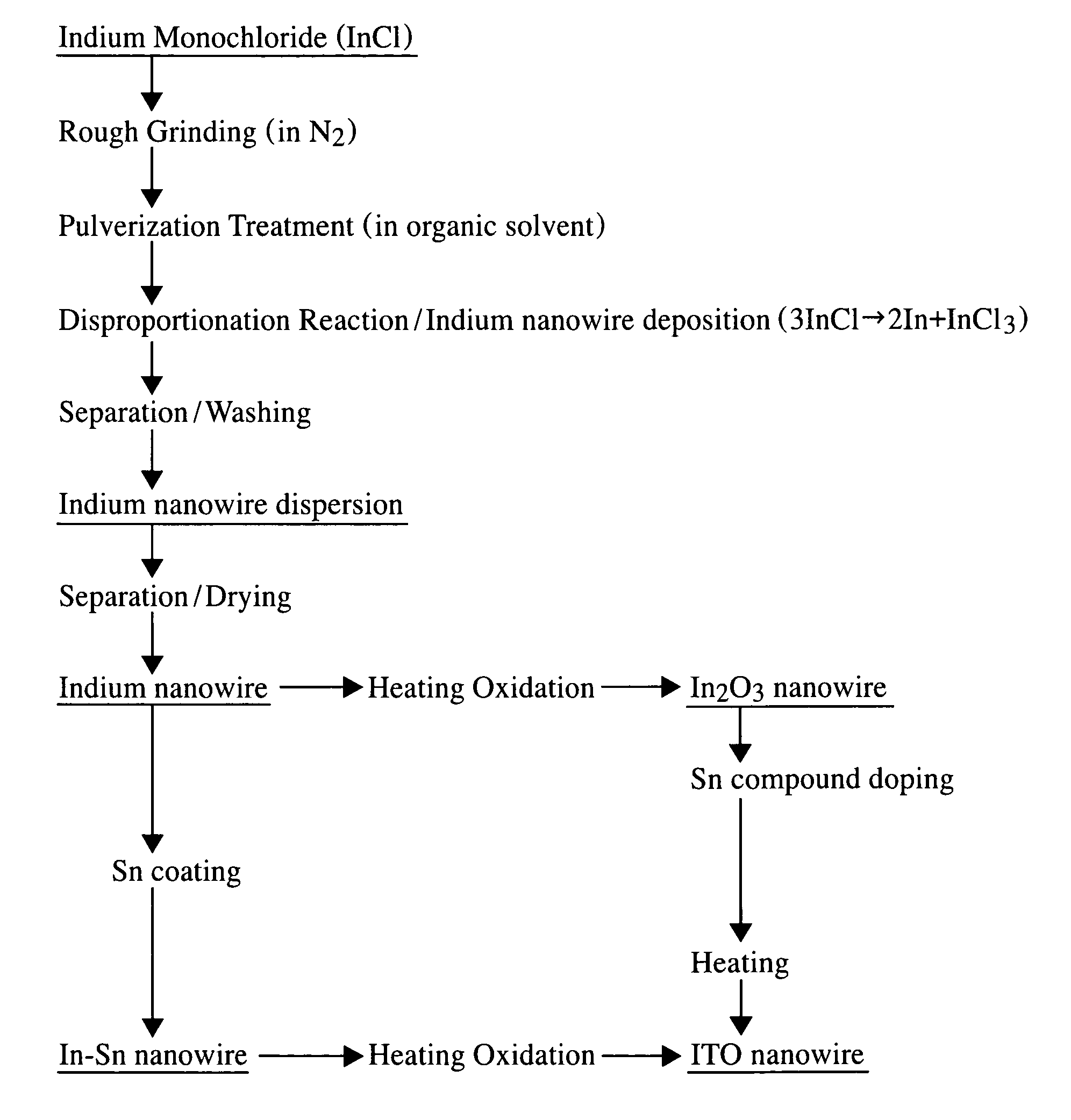
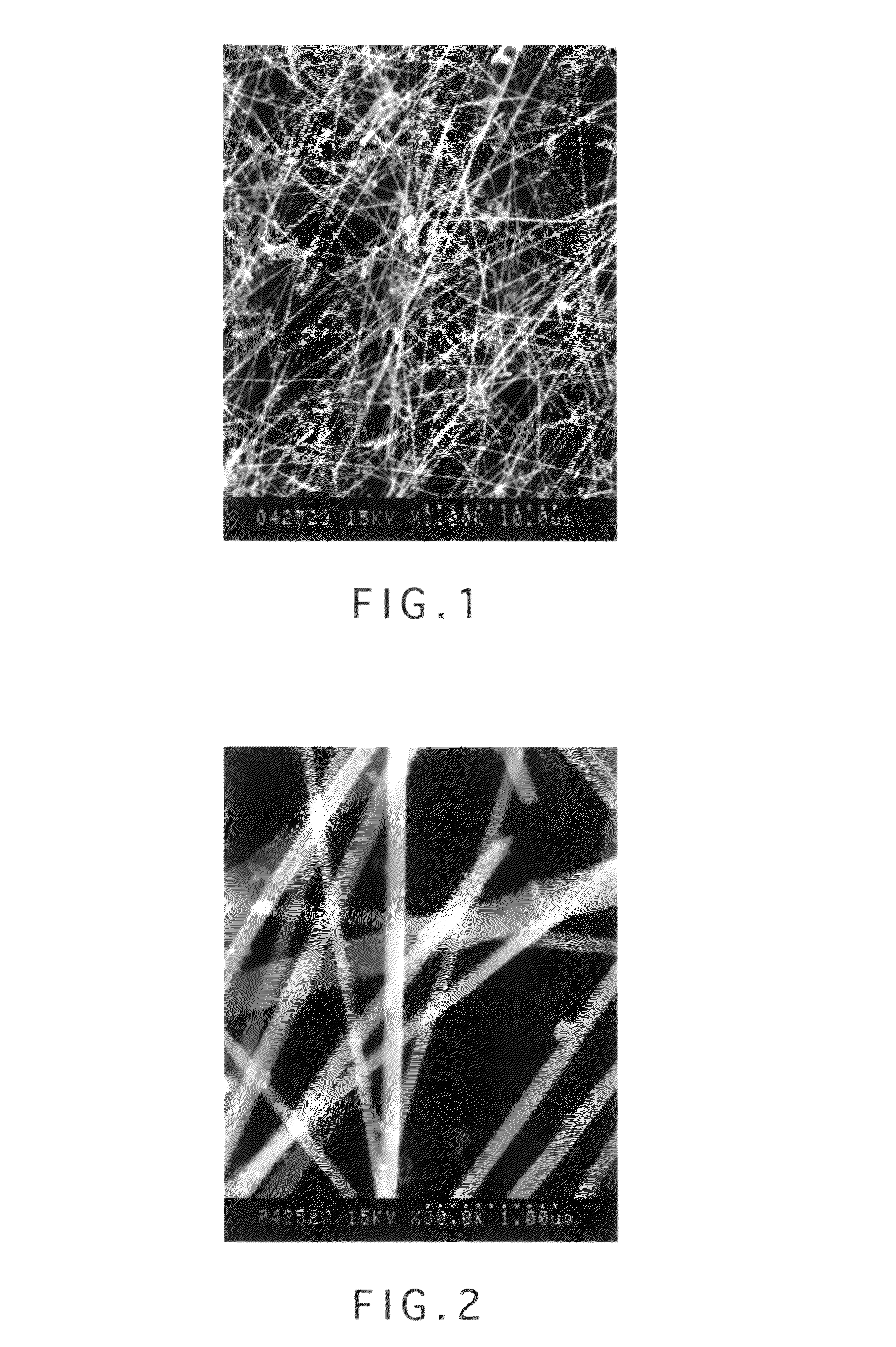
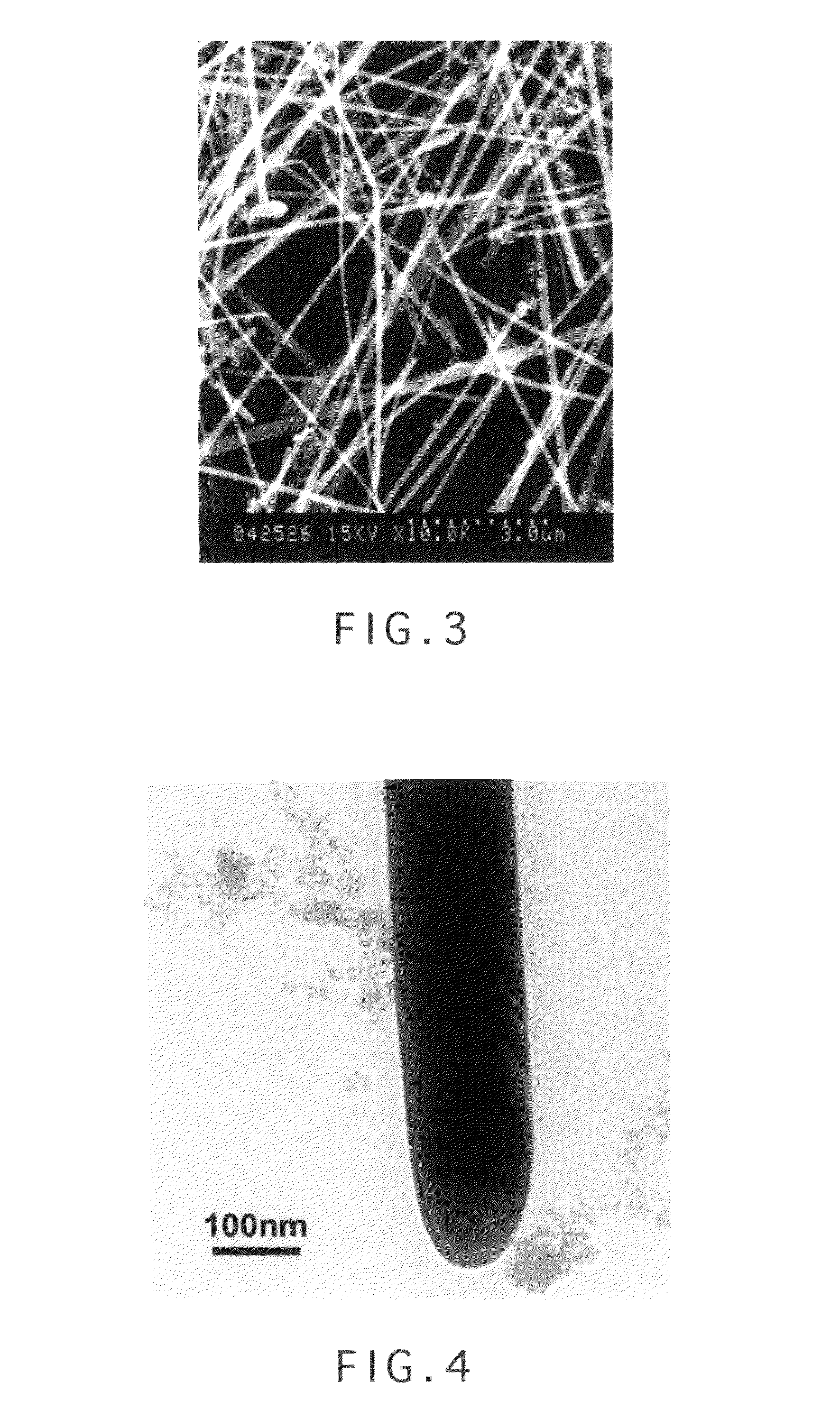
[0077]16 g of indium monochloride (InCl) powder sieved through 42 mesh (sieve opening: 355 μm) was mixed with 128 g of propylene glycol monomethyl ether acetate (PGMEA) and 0.4 g of a polymer dispersant (S36000 made by Avecia), followed by a pulverization treatment by a paint shaker adopting zirconia beads having diameters of 0.3 mm, thereby obtaining a dispersion of InCl fine particles having a particle diameter distribution between about 20 and 80 nm.

[0078]While 70 g of the dispersion of InCl fine particles was kept stirred, 70 g of ethanol was firstly added thereto, and 70 g of pure water was then gradually added to conduct a disproportionation reaction of the InCl fine particles, thereby obtaining a reacted solution containing indium nanowires (indium nanofibers). Since indium nanowires in the reacted solution gradually sedimented, there were repeatedly conducted operations to remove a supernatant after decantation, to add ethanol, and to stir the remaining solution, in a manner...

example 2

[0084]The indium nanowires obtained in Example 1 were subjected to a heat treatment (at 200° C. for 60 minutes, and then at 400° C. for 60 minutes) in the atmospheric air to cause oxidation of indium, thereby obtaining an indium oxide nanowire product comprising indium oxide nanowires according to Example 2.

[0085]The obtained indium oxide nanowires appeared to be a light yellow powder, and were confirmed to comprise indium oxide from a result of X-ray diffraction analysis. Further, it was confirmed that the nanowires kept shapes of indium nanowires before oxidation as they were, from a result of scanning electron microscope (SEM) observation (see FIG. 6).

example 3

[0086]Added into the indium-nanowire-containing ethanol solution obtained in Example 1 was an aqueous solution of tin chloride (SnCl4.xH2O), followed by addition of an aqueous solution of sodium borohydride to cause a reduction reaction, to thereby conduct coating of tin onto surfaces of the indium nanowires. Thereafter and similarly to Example 1, there were repeatedly conducted operations to remove a supernatant after decantation, to add ethanol, and to stir the remaining solution, in a manner to progress removal of reaction products other than indium nanowires coated with tin, followed by filtering separation and drying, to obtain a tin-containing indium nanowire product comprising tin-containing indium nanowires according to Example 3.

[0087]The content of tin was 0.02 mole relative to 1 mole of metal indium. Further, it was confirmed that the tin-containing indium nanowires kept shapes of indium nanowires before tin coating as they were, from a result of scanning electron microsc...


PUM

PropertyMeasurementUnit
inclination angleaaaaaaaaaa
diametersaaaaaaaaaa
diametersaaaaaaaaaa

Abstract

A production method of an indium-based nanowire product comprising indium-based nanowires according to the present invention is characterized in that the method comprises the step of: disproportionation-reacting particles including indium subhalide as main components in a nonaqueous solvent, to obtain nanowires including metal indium as main components. The electroconductive oxide nanowire product comprising electroconductive oxide nanowires of the present invention can be obtained by: subjecting, the indium nanowires additionally doped with doping metals, to a heating oxidation treatment; or doping oxides of doping metals into indium oxide nanowires obtained from the indium-based nanowires.

Description

TECHNICAL FIELD[0001]The present invention relates to an indium-based nanowire product, an oxide nanowire product, and an electroconductive oxide nanowire product, as well as production methods thereof, and more particularly to: an indium-based nanowire product and an electroconductive oxide nanowire product (hereinafter called “indium-based nanofiber product” and “electroconductive oxide nanofiber product”, respectively, as the case may be) each including nanowires having an averaged thickness in a nano-size and having wire shapes with a ratio of averaged length to averaged thickness (i.e., aspect ratio) of 30 or more in a manner to be exemplarily utilized as electroconductive fillers of various transparent electroconductive films, and as nano-wirings; as well as production methods for expediently and inexpensively producing the indium-based nanowire product and the electroconductive oxide nanowire product, respectively.BACKGROUND ART[0002]Typically, transparent electroconductive f...

Claims


Application Information

Patent Timeline
Patent Type & Authority Patents(United States)
IPC IPC(8): C22B58/00B82B1/00B22F1/00
CPCB22F1/0025B82Y30/00C01G15/00C01G19/00C04B35/62231C04B35/6261C04B35/6265C04B35/63488C30B7/00C30B29/02C30B29/60D01F9/08B22F9/30Y10T428/298C01P2004/03C01P2004/04C01P2004/16C01P2006/40C04B2235/3217C04B2235/3232C04B2235/3244C04B2235/3258C04B2235/3284C04B2235/3286C04B2235/3287C04B2235/3293C04B2235/444C04B2235/526C04B2235/5264C04B2235/9661Y10S977/762Y10S977/817B22F1/0547
Inventor YUKINOBU, MASAYA
Owner SUMITOMO METAL MINING CO LTD
Why Eureka
Try Eureka