finFETS and methods of making same

a technology of micro-fluidic transistors and transistors, applied in the field of micro-fluidic transistors, can solve problems such as increased parasitic resistan

Active Publication Date: 2011-10-25
AURIGA INNOVATIONS INC
View PDF4 Cites 91 Cited by
  • Summary
  • Abstract
  • Description
  • Claims
  • Application Information

AI Technical Summary

Problems solved by technology

However an issue with finFETs is increased parasitic resistance as the fin width is scaled down in size.

Method used


Image

  • finFETS and methods of making same
  • finFETS and methods of making same
  • finFETS and methods of making same

Examples


Embodiment Construction

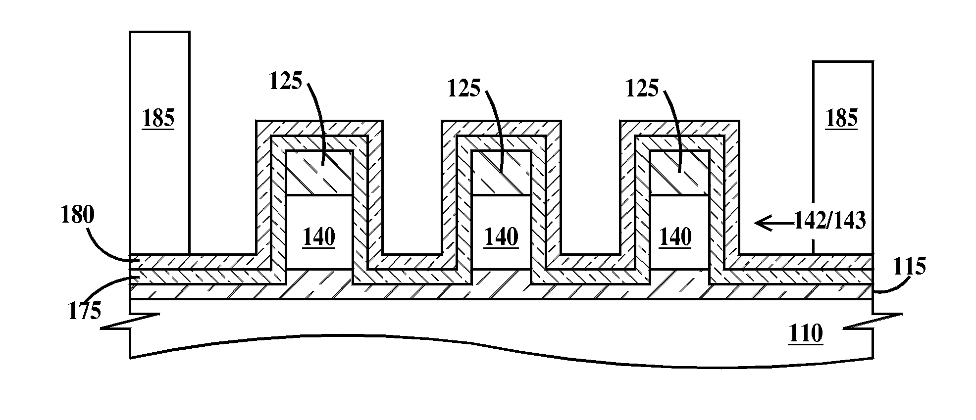
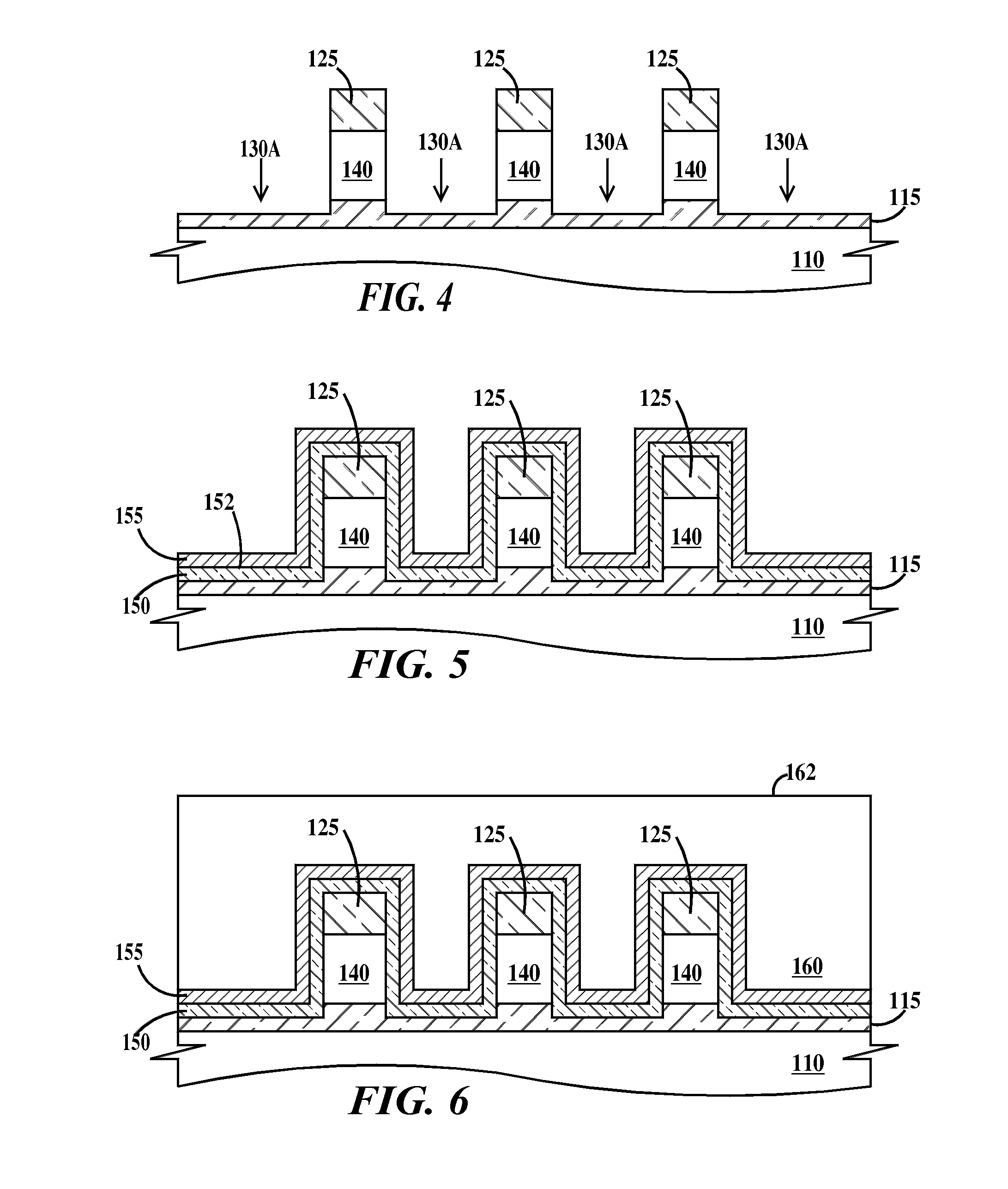
FinFETs are less susceptible to short-channel-effect (SCE) because of the ability to form double-gated devices. However, as fin sizes decrease the parasitic resistance Rext does not scale. The present invention uses multi-fin devices having merged source / drains to reduce the Rext. The embodiments of the present invention “merge” fins using epitaxial growth, but minimizes Rext and parasitic capacitance Cov, by minimizing total source-drain height so the fins merge predominately by epitaxial growth from the silicon substrate instead of the from fin sidewall. This requires the use of thinner than normal buried oxide layers in the silicon-on-insulator (SOI) substrates on which the finFETs are fabricated.

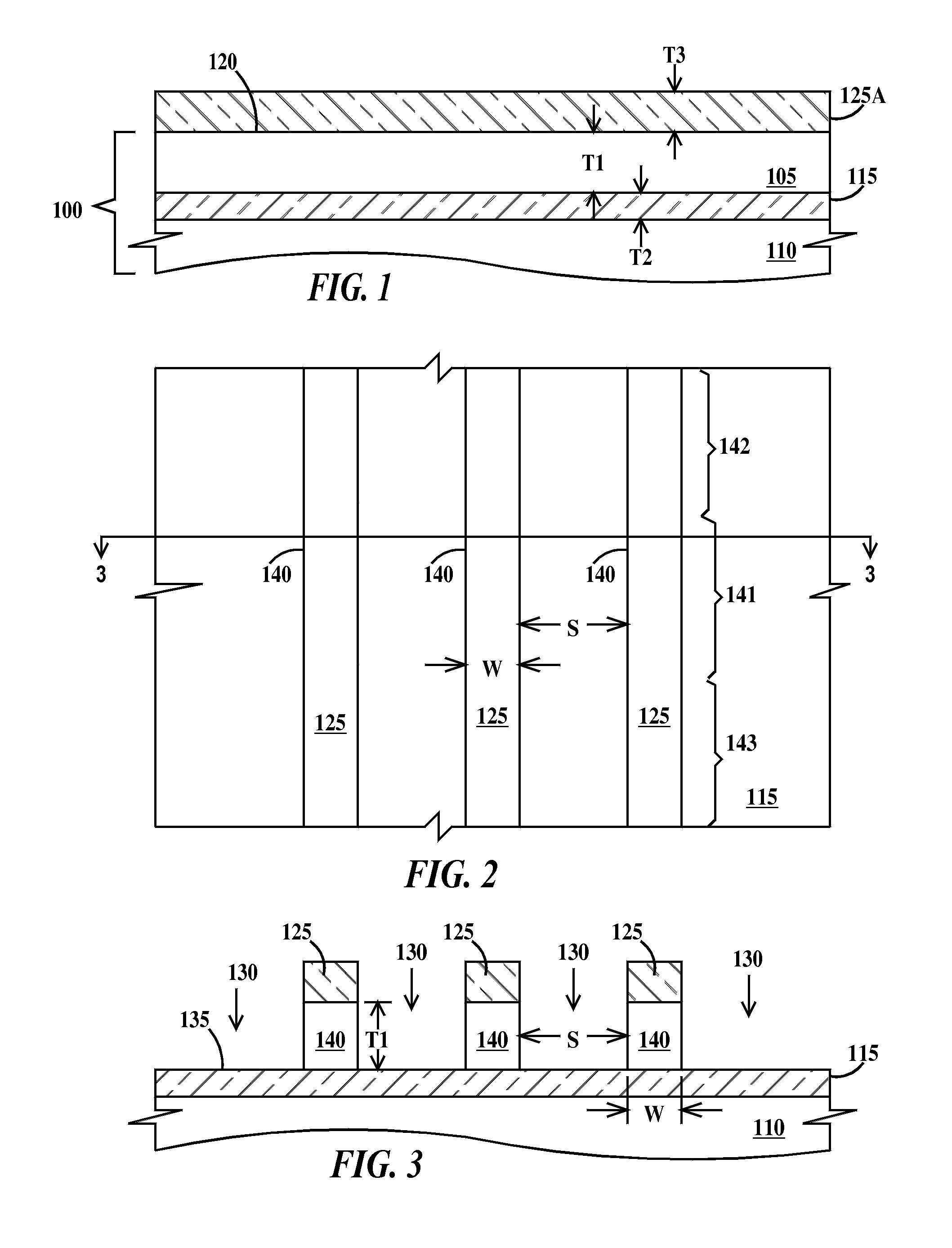
FIGS. 1 through 20 illustrate fabrication of finFETs according to embodiments of the present invention. FIG. 1 is a cross-sectional view of a starting substrate for fabrication of a merged-fin finFET. In FIG. 1, an SOI substrate 100 includes a single-crystal silicon layer 105 separated f...


PUM

PropertyMeasurementUnit
thicknessaaaaaaaaaa
thicknessaaaaaaaaaa
diametersaaaaaaaaaa

Abstract

A method of fabricating and a structure of a merged multi-fin finFET. The method includes forming single-crystal silicon fins from the silicon layer of an SOI substrate having a very thin buried oxide layer and merging the end regions of the fins by growing vertical epitaxial silicon from the substrate and horizontal epitaxial silicon from ends of the fins such that vertical epitaxial silicon growth predominates.

Description

FIELD OF THE INVENTIONThe present invention relates to the field of semiconductor transistors; more specifically, it relates to finFETs and methods of fabricating finFETs.BACKGROUND OF THE INVENTIONFin field effect transistors (finFETs) are a leading candidate to replace planer metal-oxide-silicon field effect transistors (MOSFETs). However an issue with finFETs is increased parasitic resistance as the fin width is scaled down in size. Accordingly, there exists a need in the art to mitigate the deficiencies and limitations described hereinabove.SUMMARY OF THE INVENTIONA first aspect of the present invention is a method, comprising: (a) forming two or more silicon fins on a top surface of an insulating layer on a silicon substrate, each fin of the two or more fins having a central region between and abutting first and second end regions and opposite sides; (b) forming a gate dielectric layer on the opposite sides of each fin of the two or more fins; (c) forming an electrically conduc...

Claims


Application Information

Patent Timeline
Patent Type & Authority Patents(United States)
IPC IPC(8): H01L21/00
CPCH01L29/66795H01L29/785
Inventor CHAN, KEVIN K.KANARSKY, THOMAS SAFRONLI, JINGHONGOUYANG, CHRISTINE QIQINGPARK, DAE-GYUREN, ZHIBINWANG, XINHUIYIN, HAIZHOU
Owner AURIGA INNOVATIONS INC
Why Eureka
Try Eureka