Semiconductor device and manufacturing method thereof, SOI substrate and display device using the same, and manufacturing method of the SOI substrate

a semiconductor and semiconductor technology, applied in the field of semiconductor devices, can solve the problems of deterioration of tft property reproducibility, insufficient transistor performance to form a high-performance device of si, and cracks in films, etc., to achieve the effect of improving bond strength, increasing s coefficient, and reducing mobility

Inactive Publication Date: 2007-03-22
SHARP KK
View PDF19 Cites 111 Cited by
  • Summary
  • Abstract
  • Description
  • Claims
  • Application Information

AI Technical Summary

Benefits of technology

[0021] Another object of the present invention is to provide a semiconductor device constituted of a large size and inexpensive substrate in which a single crystal Si thin film is provided and its property is stabilized.
[0084] With the foregoing configuration, it is possible to obtain advantages similar to those of the foregoing manufacturing methods.

Problems solved by technology

This is because the polycrystalline Si brings about the following problems: because of (a) a localized state in the band gap that is caused by incomplete crystallization, (b) deficiency in the vicinity of a crystal grain boundary, drop in the mobility that is caused by the presence of the localized state in the band gap, and (d) increase in an S coefficient (sub-threshold coefficient), performance of the transistor is too insufficient to form a high-performance device of Si.
Thus, generally, a tensile stress of approximately 109 Pa is exerted on the Si film, so that there occur such problems: cracks appear in the film, reproducibility in the TFT property is deteriorated, non-uniformity is large, and the like.
However, when the single crystal Si thin film is to be bonded to an insulating substrate other than the Si substrate, for example, a glass substrate or a quartz substrate, there occurs such problem that Si is stripped because of a thermal-expansion-coefficient difference between Si and the insulating substrate such as the quartz substrate.
This is because the polycrystalline Silicon film brings about the following problem: because of (a) a localized state in the band gap that is caused by incomplete crystal, (b) drop in the mobility, or (c) increase in a sub-threshold coefficient (S coefficient) that are brought about by the presence of the localized state in the band gap in the vicinity of a crystal grain boundary, performance of the transistor is too insufficient to form a high-performance device of silicon.
Thus, crystals are severely damaged, so that there occur the following problems: it is impossible to obtain sufficient property of the single crystal, or it is impossible to obtain complete insulating property because of deviation from stoichiometry of a silicon dioxide film portion.
Thus, it is impossible to manufacture large size liquid crystal display panel and organic EL panel.
In a case of a small size panel, the manufacturing cost becomes high, and it is difficult to use the technique in practice.
Further, in a case where a stress is exerted on a bonded interface, the TFT property is deteriorated because of differences and non-uniformity in the stress exerted on the interface.
Further, in the prior art, it is considered that: when the single crystal silicon substrate is bonded, it is impossible to obtain the sufficient bond strength unless exposed in a high temperature.
Thus, a temperature for performing the heating process is 800° C. to 1200° C. It is considered that a high-heat-resistant crystallized glass whose strain point is not less than 750° C. is suitable, so that there occurs the following problem: the technique cannot be applied to a high-strain-point nonalkali glass, typically used in a liquid crystal panel of the active matrix driving, whose strain point is not more than 700° C.

Method used


Image

  • Semiconductor device and manufacturing method thereof, SOI substrate and display device using the same, and manufacturing method of the SOI substrate
  • Semiconductor device and manufacturing method thereof, SOI substrate and display device using the same, and manufacturing method of the SOI substrate
  • Semiconductor device and manufacturing method thereof, SOI substrate and display device using the same, and manufacturing method of the SOI substrate

Examples


embodiment 2

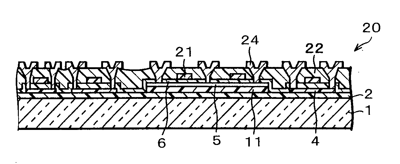
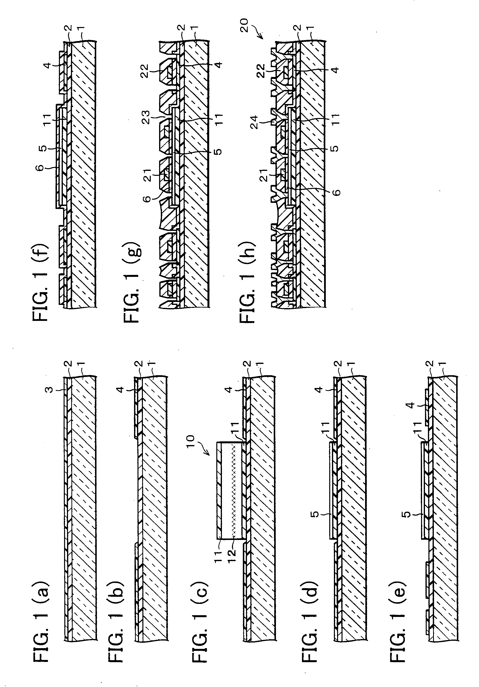
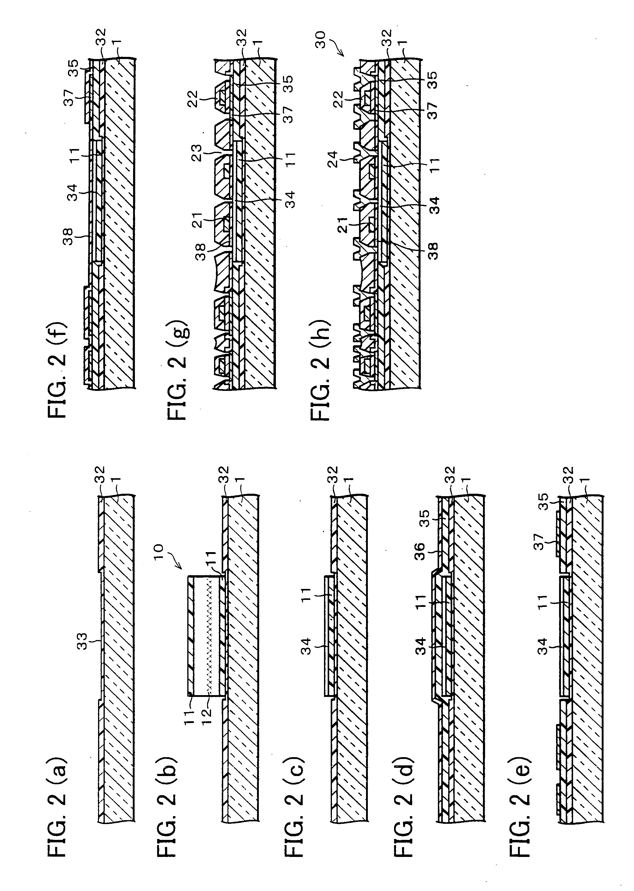
[0134] The following description will discuss an active matrix substrate 30 using a TFT as another embodiment of the present invention referring to FIG. 2(h). Note that, as to the same members as in the active matrix substrate 20 of Embodiment 1, description thereof will be omitted.

[0135] The active matrix substrate 30 which functions as a semiconductor device includes: an insulating substrate 1; SiO2 (silicon oxide) films 32 and 11; a second SiO2 film 35; a polycrystalline Si thin film 37; a single crystal Si thin film 34; a gate oxide film 38; a gate electrode 21; an interlayer insulating film 22; and a metal wiring 24.

[0136] As the insulating substrate 1, #1737 (trade name, alkaline earth-alumino boro-silicated glass, made by Corning Incorporated) which is a high-strain-point glass is used.

[0137] The SiO2 film 32 having an approximately 350 nm is formed on an entire surface of the insulating substrate 1.

[0138] The second SiO2 film 35 having an approximately 100 nm thickness i...

embodiment 3

[0156] The following description will discuss an active matrix substrate using a TFT as still another embodiment of the present invention. A cross sectional structure of the active matrix substrate is arranged in the same manner as in the active matrix substrate 20 of Embodiment 1, so that only differences between the active matrix substrate of the present embodiment and the active matrix substrate 20 of Embodiment 1 are described.

[0157] A polycrystalline Si thin film 43 (see FIG. 3(d)) of the present embodiment is constituted of polycrystalline Si whose crystal-growing directions are uniformed, and are uniformed, that is, so-called continuous grain silicon Si.

[0158] An N channel TFT formed in a conventional continuous grain silicon Si area was such that its mobility was approximately 200 cm2 / V·sec. On the other hand, in the liquid crystal display active matrix substrate, the N channel TFT formed in the single crystal Si area is such that the mobility is approximately 500 cm2 / V·se...

embodiment 4

[0172] The following description will discuss an active matrix substrate 50 using a TFT as another embodiment of the present invention. The active matrix substrate 50 is arranged substantially in the same manner as in the active matrix substrate 20 of Embodiment 1, so that only differences between the active matrix substrate 50 and the active matrix substrate 20 are described.

[0173] A thickness of the SiO2 film 2 in the active matrix substrate 20 is approximately 200 nm. On the other hand, a thickness of an SiO2 film 52 in the active matrix substrate 50 of the present embodiment is approximately 350 nm, and there is formed a concaved portion 55 (see FIG. 4(b)) having an approximately 150 nm depth.

[0174] Further, a thickness of the SiO2 film 11 of the active matrix substrate 20 is approximately 200 nm. On the other hand, a thickness of an SiO2 film 61 of the active matrix substrate 50 of the present embodiment is approximately 400 nm.

[0175] An N channel TFT formed in a conventiona...


PUM

PropertyMeasurementUnit
temperatureaaaaaaaaaa

Abstract

A polycrystalline Si thin film and a single crystal Si thin film are formed on an SiO2 film deposited on an insulating substrate. A polycrystalline Si layer is grown by thermally crystallizing an amorphous Si thin film so as to form the polycrystalline Si thin film. A single crystal Si substrate, having (a) an SiO2 film thereon and (b) a hydrogen ion implantation portion therein, is bonded to an area of the polycrystalline Si thin film that has been subjected to etching removal, and is subjected to a heating process. Then, the single crystal Si substrate is divided at the hydrogen ion implantation portion in an exfoliating manner, so as to form the single crystal Si thin film. As a result, it is possible to provide a large-size semiconductor device, having the single crystal Si thin film, whose property is stable, at a low cost.

Description

FIELD OF THE INVENTION [0001] The present invention relates to a semiconductor device and to a manufacturing method thereof, and particularly relates to a semiconductor device having an integrated circuit constituted of plural MOSs and to a manufacturing method thereof. [0002] Further, the present invention relates to an SOI substrate constituted by (a) bonding a single crystal silicon thin film in which hydrogen ions have been implanted to a substrate and (b) dividing the single crystal silicon thin film at a hydrogen ion implantation portion, and the present invention further relates to a semiconductor device using the SOI substrate, and to a manufacturing method of the SOI substrate. [0003] In addition, the present invention relates to a semiconductor device, used in an active matrix driving liquid crystal display device and the like, that improves circuit performance of a device in which peripheral driving circuits, a control circuit, and the like are integrated. BACKGROUND OF T...

Claims


Application Information

Patent Timeline
Patent Type & Authority Applications(United States)
IPC IPC(8): H01L27/12H01L21/336H01L21/762H01L21/77H01L21/84H01L29/786
CPCH01L21/76254H01L2924/1305H01L27/1266H01L29/66757H01L29/78654H01L29/78675H01L29/78696H01L2221/68363H01L2224/24226H01L2924/01004H01L2924/0102H01L2924/01046H01L2924/01057H01L2924/01078H01L2924/01079H01L2924/3511H01L2924/01019H01L2924/01021H01L2924/01068H01L2924/13091H01L2924/12041H01L21/26506H01L27/1214H01L2924/00H01L27/1218H01L27/1229H01L2924/12044H01L21/20
Inventor TAKAFUJI, YUTAKAITOGA, TAKASHI
Owner SHARP KK
Why Eureka
Try Eureka