Low-temperature formation of polycrystalline semiconductor films via enhanced metal-induced crystallization

a technology of enhanced metal crystallization and low temperature, applied in the direction of polycrystalline material growth, crystal growth process, coating, etc., can solve the problems of unsuitable poly-si film formation on low-cost glass and plastic substrates, unsatisfactory, various other techniques, etc., to achieve enhanced poly-si film formation, rapid crystallization, and low temperature

Active Publication Date: 2011-10-25
RGT UNIV OF CALIFORNIA
View PDF4 Cites 8 Cited by
  • Summary
  • Abstract
  • Description
  • Claims
  • Application Information

AI Technical Summary

Benefits of technology

[0012]In utilizing the inventive method to incorporate Si (2%) into the aluminum film, the temperature required for aluminum-induced crystallization of amorphous silicon is reduced by more than 100° C. Consequently, polycrystalline silicon films can be formed even at temperatures below 300° C., making the process compatible with low-cost glass substrates, plastic substrates and substrates containing complementary metal-oxide-semiconductor (CMOS) integrated circuits. Many applications exist which can benefit from the ability to form polycrystalline semiconductor at reduced temperatures, such as at or below the range from about 300° C. to 350° C. It will also be appreciated that the formation of polycrystalline material by the inventive method is enhanced even at higher temperature regimes, wherein one can lower temperature or achieve more rapid crystallization.
[0017]The method may be utilized to form polycrystalline semiconductor material selected from the group of Si, Ge, Si1-xGex, Si1-yCy, SiC, and others. The method lowers the temperature required for metal-induced crystallization, such as lowering it by at least approximately 50° C. The small percentage of semiconductor material needed is less than 10 atomic percent, and preferably comprises between 0.5 to 5 atomic percent of semiconductor material, and most preferably about 2 atomic percent. Pulsed excimer laser annealing (ELA) can be utilized separately, or in conjunction with a more conventional isothermal annealing step.

Problems solved by technology

Use of such a high process temperature renders this approach unsuitable for formation of poly-Si films on low-cost glass and plastic substrates and on substrates with completed CMOS integrated circuits.
Various other techniques have been attempted, with less than ideal results, toward crystallizing amorphous silicon films without subjecting the material to excessive temperatures for the given application.

Method used


Image

  • Low-temperature formation of polycrystalline semiconductor films via enhanced metal-induced crystallization
  • Low-temperature formation of polycrystalline semiconductor films via enhanced metal-induced crystallization
  • Low-temperature formation of polycrystalline semiconductor films via enhanced metal-induced crystallization

Examples


Embodiment Construction

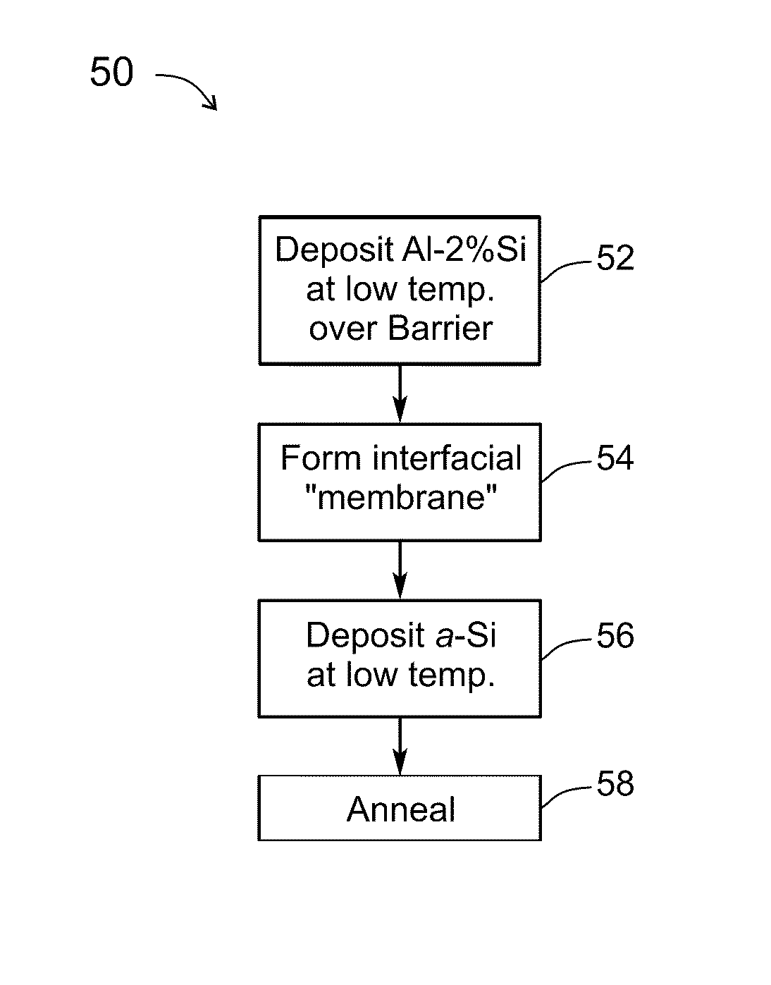
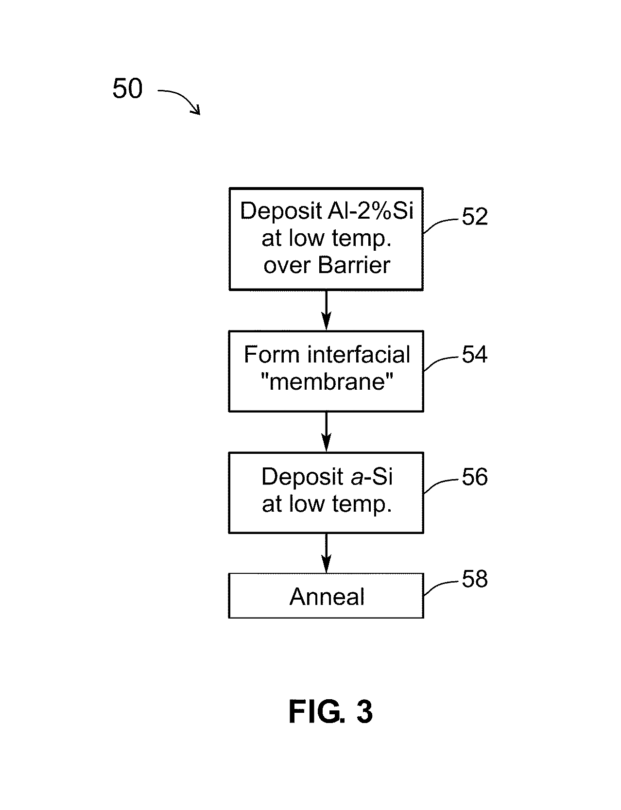
[0048]Referring more specifically to the drawings, for illustrative purposes the present invention is embodied in the apparatus generally shown in FIG. 1 through FIG. 14. It will be appreciated that the apparatus may vary as to configuration and as to details of the parts, and that the method may vary as to the specific steps and sequence, without departing from the basic concepts as disclosed herein.

[0049]1. Introduction

[0050]The invention provides a method by which the temperature required to form polycrystalline semiconductor films can be reduced to temperatures at or even below 300° C., thus opening many new application areas. Benefits are provided over conventional metal-induced crystallization in response to inclusions of small percentages of semiconductor within the metal material.

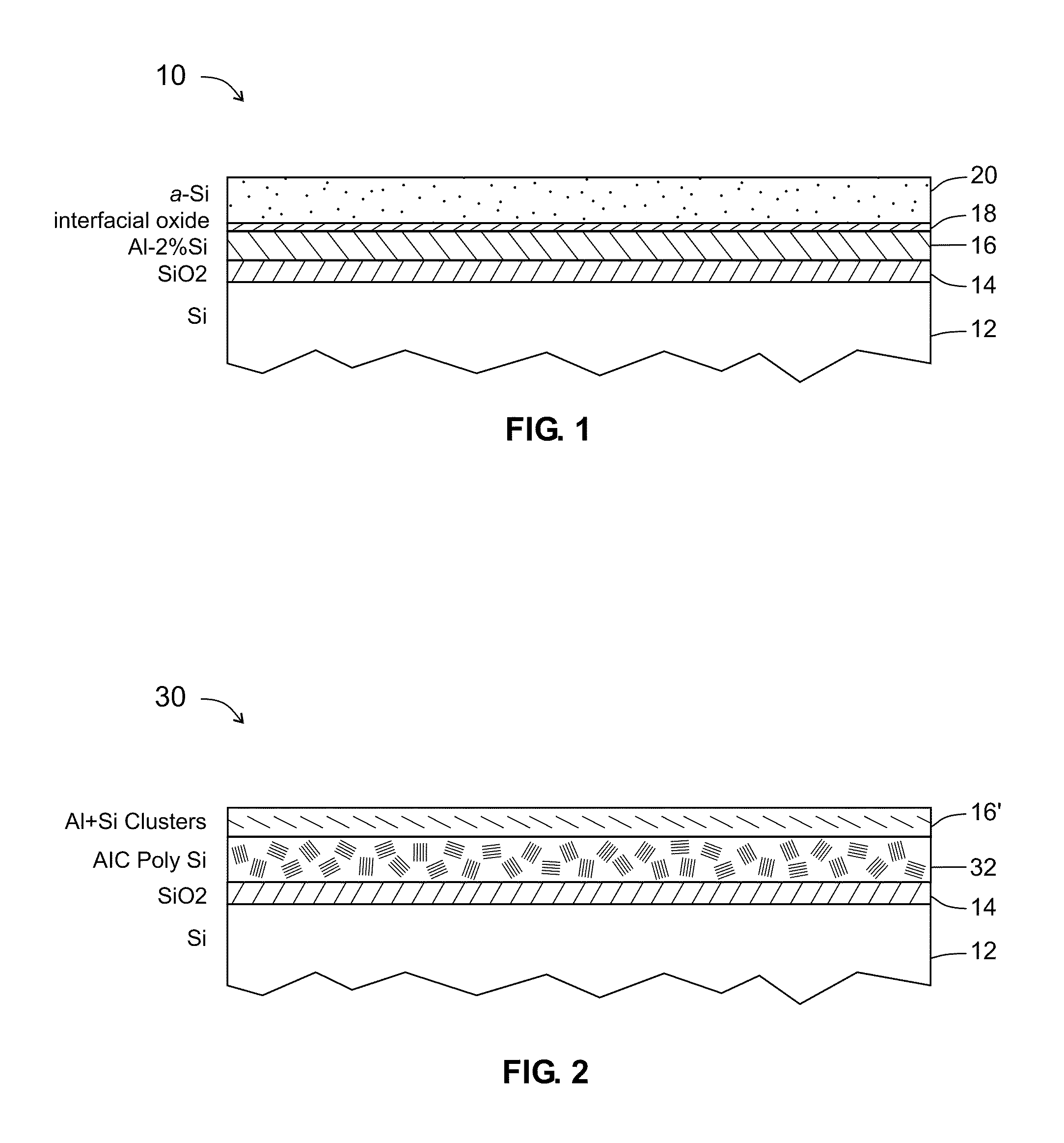
[0051]FIG. 1 illustrates an embodiment 10 of material layers shown in cross-section which have been deposited preparatory to forming the polycrystalline semiconductor, which by way of example is pol...


PUM

PropertyMeasurementUnit
temperatureaaaaaaaaaa
temperaturesaaaaaaaaaa

Abstract

A method for forming polycrystalline semiconductor film from amorphous semiconductor film at reduced temperatures and / or accelerated rates. The inclusion of a small percentage of semiconductor material, such as 2% within the metal layer, reduces the temperatures required for crystallization of the amorphous semiconductor by at least 50° C. in comparison to the use of the metal layer without the small percentage of semiconductor material. During a low temperature isothermal annealing process adjacent Al-2% Si and a-Si films undergo a layer exchange resulting in formation of a continuous polycrystalline silicon film having good physical and electrical properties. Formation of polycrystalline-semiconductor in this manner is suitable for use with low temperature substrates (e.g., glass, plastic) as well as with numerous integrated circuit and MEMs fabrication devices and practices.

Description

CROSS-REFERENCE TO RELATED APPLICATIONS[0001]This application claims priority from, and is a 35 U.S.C. §111(a) continuation of, PCT international application serial number PCT / US2008 / 071809, filed on Jul. 31, 2008, incorporated herein by reference in its entirety, which claims priority from U.S. provisional application Ser. No. 60 / 953,117 filed on Jul. 31, 2007, incorporated herein by reference in its entirety.[0002]This application is also related to PCT International Publication No. WO 2009 / 018472 published on Feb. 5, 2009, incorporated herein by reference in its entirety.STATEMENT REGARDING FEDERALLY SPONSORED RESEARCH OR DEVELOPMENT[0003]This invention was made with Government support under Grant No. DMI-0304209 awarded by the National Science Foundation. The Government has certain rights in this invention.INCORPORATION-BY-REFERENCE OF MATERIAL SUBMITTED ON A COMPACT DISC[0004]Not ApplicableNOTICE OF MATERIAL SUBJECT TO COPYRIGHT PROTECTION[0005]A portion of the material in this...

Claims


Application Information

Patent Timeline
Patent Type & Authority Patents(United States)
IPC IPC(8): H01L21/20
CPCH01L21/02529H01L21/02532H01L21/02672H01L21/02686H01L21/823828C30B1/023C30B29/06
Inventor MABOUDIAN, ROYADELRIO, FRANK W.LAI, JOANNALIU, TSU-JAE KING
Owner RGT UNIV OF CALIFORNIA
Why Eureka
Try Eureka