Integrated circuit cell architecture configurable for memory or logic elements

a cell architecture and integrated circuit technology, applied in the field of integrated circuit cell architecture, can solve the problems of low power consumption, low non-recurring expense, and low performance of fpgas, and achieve the effects of low non-recurring expense, lower power consumption, and improved performan

Inactive Publication Date: 2011-10-25
AVAGO TECH INT SALES PTE LTD
View PDF15 Cites 112 Cited by
  • Summary
  • Abstract
  • Description
  • Claims
  • Application Information

AI Technical Summary

Benefits of technology

[0014]The improved layout architecture can achieve interconnection of transistors having different sizes within each layout cell. Moreover, interconnection can be achieved across cells to form basic logic gates as well as more complex digital and analog subsystems. In addition, each cell contains a layout of transistors that can be variably coupled to achieve a memory cell. In particular, the memory cell can comprise a cross-coupled pair of transistors that form a latch, with pass transistors or access transistors to that latch. Preferably, no more than two cells are needed to ac...

Problems solved by technology

That is, layout is performed on a chip-by-chip basis and cannot be easily modified whenever a design change is needed for that particular product.
An ASIC thereby enjoys the benefits of high performance, but also has a fairly high non-recurring expense each time a design change is needed.
FPGAs unfortunately have lower performance and higher power consumption relative to ASIC designs, yet enjoy a lower non-recurring expense.
However, structured ASICs are not programmed in the field as in FPGAs, nor do structu...

Method used


Image

  • Integrated circuit cell architecture configurable for memory or logic elements
  • Integrated circuit cell architecture configurable for memory or logic elements
  • Integrated circuit cell architecture configurable for memory or logic elements

Examples


Embodiment Construction

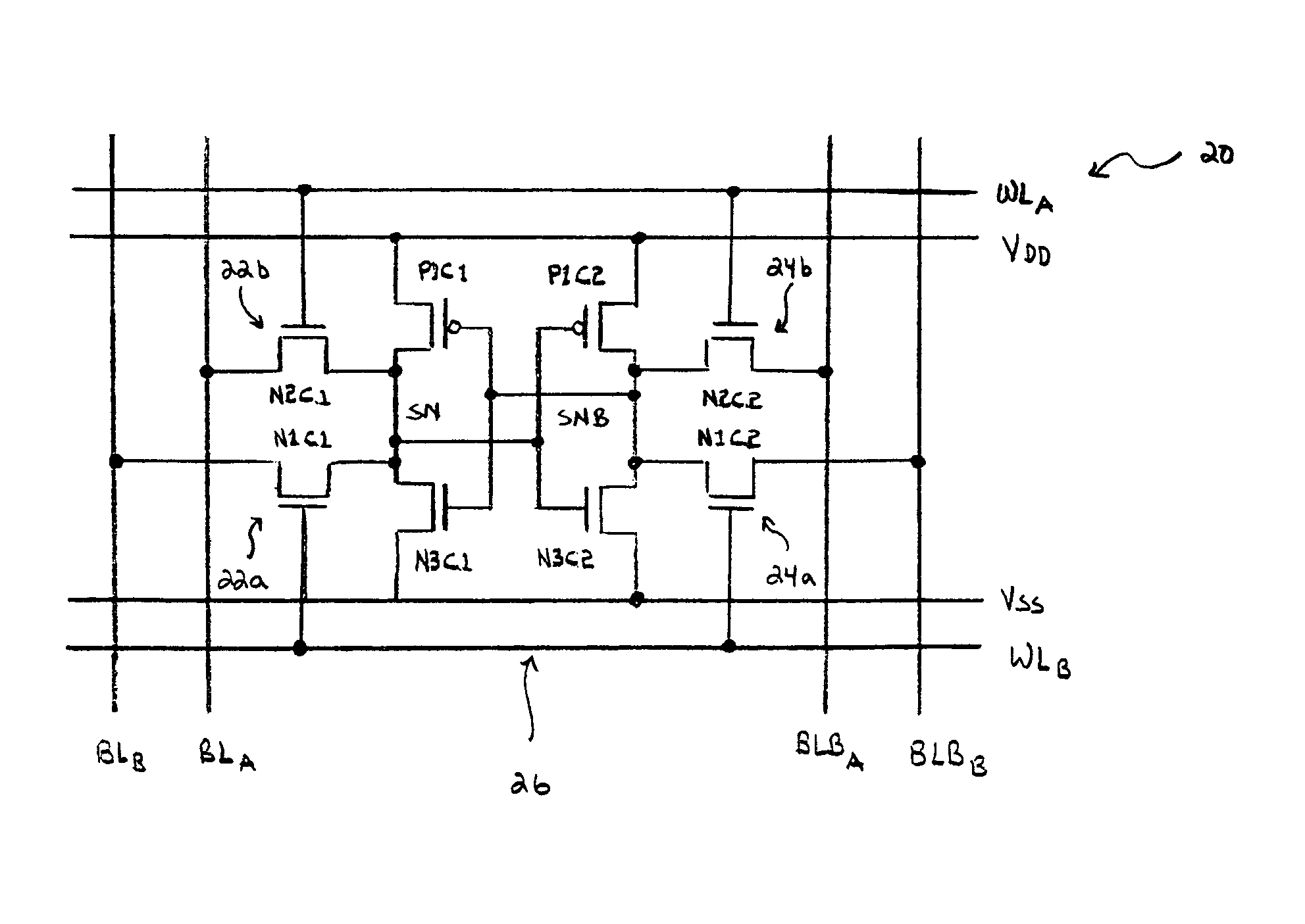
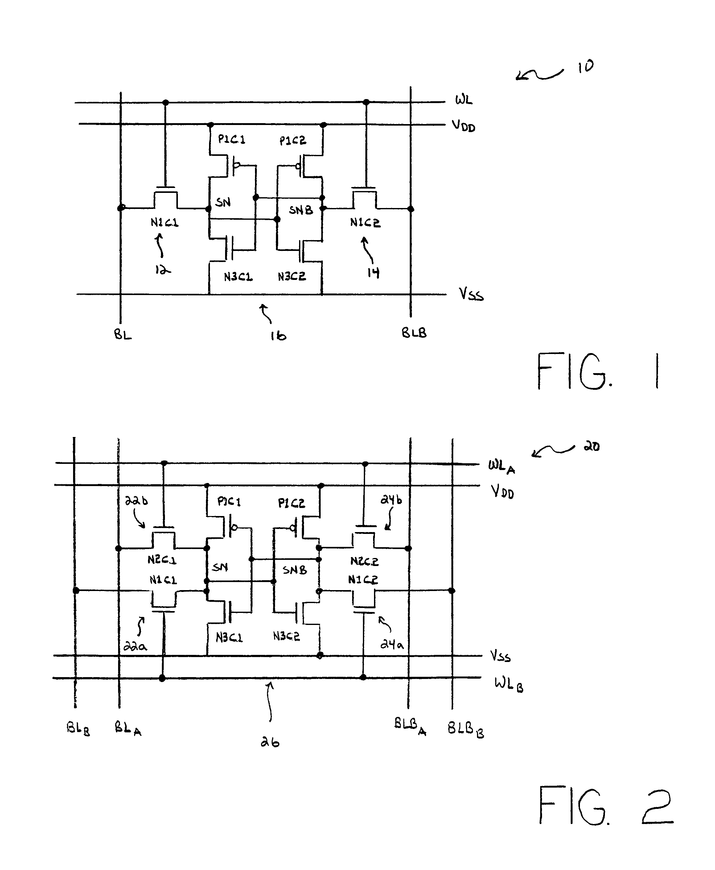
[0029]Turning now to the drawings, FIG. 1 illustrates a memory cell 10. Memory cell 10 is shown as a SRAM cell. However, it is contemplated that the use of the term “memory cell” includes any type of memory cell that can receive written logic values and transmit read logic values that are stored in the interim. Popular forms of memory cells include SRAM, non-volatile cells, DRAM, etc.

[0030]Memory cell 10 can be accessed by applying a voltage to the wordline (WL) which activates access transistors 12 and 14. Accessing transistors 12 and 14 will cause one of two bit lines BL or BLB to sense the contents of the memory cell based on the voltages present at the storage nodes SN and SNB. For example, if storage node SN is at a high logic value and node SNB is at a low logic value when the wordline is raised, the cross-coupled pairs of inverters 16 read out the latched values at SN and SNB onto bit lines BL and BLB. The state of the memory cell (either a logic 1 or a logic 0 voltage value)...


PUM


Abstract

An improved integrated circuit cell architecture is provided for configurability between a memory cell or logic elements. The cell architecture is configured on variable layers above a first layer of metal, with the first layer of metal and layers therebelow reserved as fixed layers. By coupling a maximum of two layout cells together, a single-port or dual-port memory cell is realized. Likewise, by interconnecting transistors within a single cell or transistors among two or more cells, a logic device is realized. Within each cell, the bit lines are arranged on a layer separate from the wordlines, and extend orthogonal to each other.

Description

BACKGROUND OF THE INVENTION[0001]1. Field of the Invention[0002]This invention relates to integrated circuits and, more particularly, to cell based integrated circuit layout architecture that is configurable as a logic device or a single / dual port memory cell using no more than two configurable cells.[0003]2. Description of the Related Art[0004]The following descriptions and examples are not admitted to be prior art by virtue of their inclusion within this section.[0005]An integrated circuit generally comprises the interconnection of various circuit elements. Those circuit elements include transistors, resistors, capacitors, logic gates, flip-flops, registers, etc. In order to achieve functionality, the various circuit elements must be interconnected with attention given to where those elements are relative to each other. For example, performance of the integrated circuit is affected by where the elements are connected, and the interconnect length between elements. Optimal performan...

Claims


Application Information

Patent Timeline
IPC IPC(8): H01L27/118
CPCG11C8/16H01L27/0207H01L27/11H01L27/1104H03K19/1733H01L27/11807Y10S257/903H10B10/00H10B10/12
Inventor VENKATRAMAN, RAMNATHMONZEL, III, CARL ANTHONYRAMESH, SUBRAMANIAN
Owner AVAGO TECH INT SALES PTE LTD
Why Eureka
Try Eureka