

Liquid crystal display device
a liquid crystal display and display device technology, applied in semiconductor devices, instruments, electrical devices, etc., can solve the problems of reducing the yield and no option other than to sacrifice the electrical characteristics of thin film transistors, and achieve the effect of reducing the number of photomasks, simplifying the manufacturing process of thin film transistors, and significantly reducing the number of steps for manufacturing thin film transistors
- Summary
- Abstract
- Description
- Claims
- Application Information
AI Technical Summary
Benefits of technology
Problems solved by technology
Method used
Image

Examples
embodiment mode 1
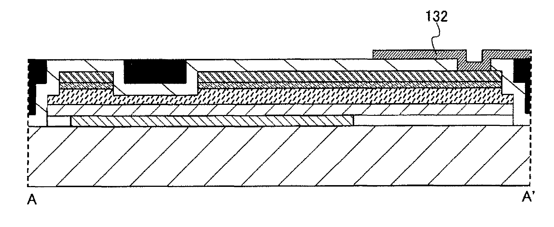
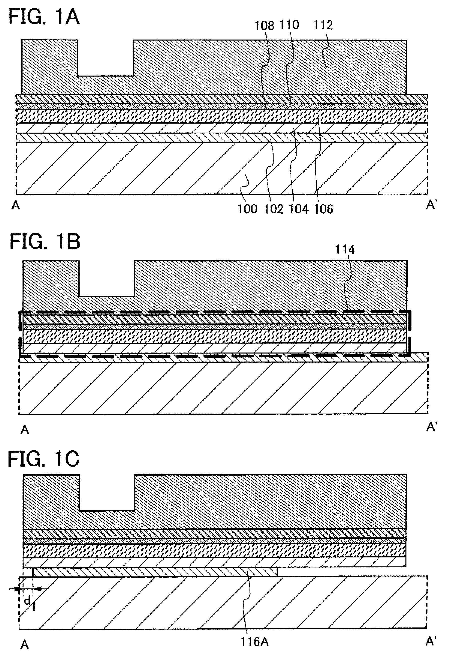
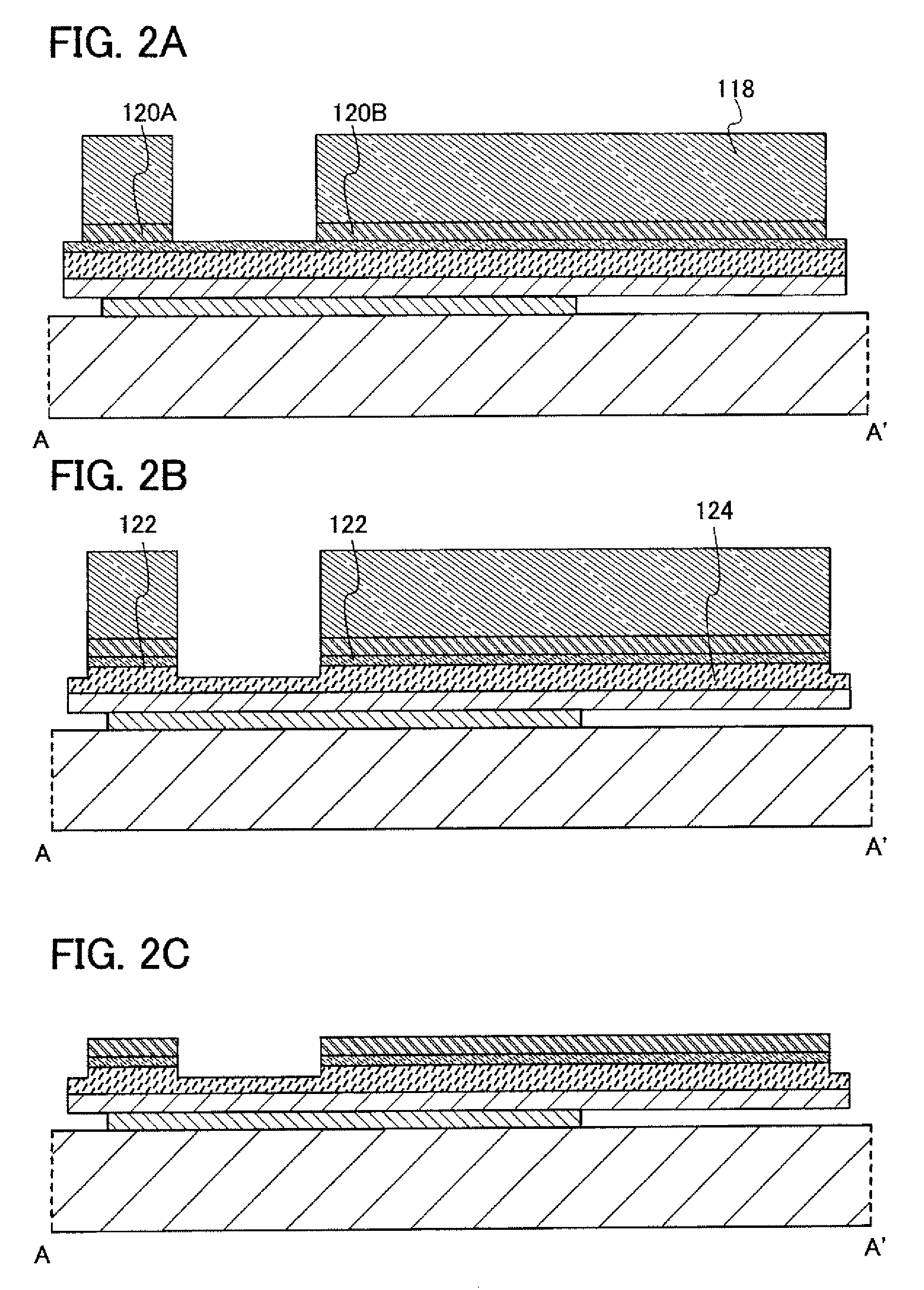
[0066]In this embodiment mode, an example of a method for manufacturing a semiconductor device will be described with reference to FIGS. 1A to 25B-2.
[0067]FIG. 16 to FIG. 20 are plan views of thin film transistors according to this embodiment mode. FIG. 20 is a drawing of the situation in which steps up to and including the step of forming a pixel electrode have been finished. FIG. 1A to FIG. 3C are cross-sectional views taken along line A-A′ in FIG. 16 to FIG. 20. FIG. 4A to FIG. 6C are cross-sectional views taken along line B-B′ in FIG. 16 to FIG. 20. FIG. 7A to FIG. 9C are cross-sectional views taken along line C-C′ in FIG. 16 to FIG. 20. FIG. 10A to FIG. 12C are cross-sectional views taken along line D-D′ in FIG. 16 to FIG. 20. FIG. 13A to FIG. 15C are cross-sectional views taken along line E-E′ in FIG. 16 to FIG. 20.
[0068]First, a first conductive film 102, a first insulating film 104, a semiconductor film 106, an impurity semiconductor film 108, and a second conductive film 11...
embodiment mode 2
[0163]In this embodiment mode, a manufacturing method of a thin film transistor and a manufacturing method of a display device according to the present invention, which are different from those of Embodiment Mode 1, will be described. Specifically, a manufacturing method of a thin film transistor which is similar to that in Embodiment Mode 1, without using a multi-tone mask will be described with reference to FIGS. 26A, 26B, and 26C, FIGS. 27A, 27B, and 27C, FIG. 28, FIG. 29, and FIG. 30.
[0164]FIGS. 26A, 26B, and 26C correspond to FIG. 1A, FIG. 1C, and FIG. 2A of Embodiment Mode 1. FIGS. 27A, 27B, and 27C correspond to FIG. 10A, FIG. 10C, and FIG. 11A of Embodiment Mode 1. FIG. 28, FIG. 29, and FIG. 30 correspond to FIG. 16, FIG. 17, and FIG. 18 of Embodiment Mode 1. The cross-sectional views taken along line A-A′ illustrated in FIG. 28, FIG. 29, and FIG. 30 correspond to FIGS. 26A, 26B, and 26C, and the cross-sectional views taken along line D-D′ illustrated in FIG. 28, FIG. 29, an...
embodiment mode 3
[0174]In this embodiment mode, a manufacturing method of a thin film transistor and a manufacturing method of a liquid crystal display device according to the present invention, which are different from those of Embodiment Modes 1 and 2, will be described. Specifically, a mode in which a first conductive film 102 is etched by the first etching which is described in Embodiment Modes 1 and 2 will be described with reference to FIGS. 31A to 31C, FIGS. 32A to 32C, FIGS. 33A to 33C, FIGS. 34A to 34C, FIGS. 35A to 35C, and FIG. 36.
[0175]FIGS. 31A to 31C correspond to FIGS. 1A to 1C of Embodiment Mode 1. FIGS. 32A to 32C correspond to FIGS. 4A to 4C of Embodiment Mode 1. FIGS. 33A to 33C correspond to FIGS. 7A to 7C of Embodiment Mode 1. FIGS. 34A to 34C correspond to FIGS. 10A to 10C of Embodiment Mode 1. FIGS. 35A to 35C correspond to FIGS. 13A to 13C of Embodiment Mode 1. FIG. 36 corresponds to FIG. 16 of Embodiment Mode 1.
[0176]First, similar to Embodiment Mode 1, a first conductive fi...
PUM
| Property | Measurement | Unit |
|---|---|---|
| transmittance | aaaaa | aaaaa |
| transmittance | aaaaa | aaaaa |
| transmittance | aaaaa | aaaaa |
Abstract
Description
Claims
Application Information