Replacement metal gate transistors with reduced gate oxide leakage

a metal gate transistor and oxide leakage technology, applied in the field of semiconductor devices, can solve the problems of adversely affecting the leakage current, affecting the objective, and affecting the engineering complexity of the semiconductor device, so as to reduce the leakage current, reduce the eot, and reduce the effect of eo

Active Publication Date: 2011-11-08
ADVANCED MICRO DEVICES INC
View PDF13 Cites 9 Cited by
  • Summary
  • Abstract
  • Description
  • Claims
  • Application Information

AI Technical Summary

Benefits of technology

[0007]An advantage of the present invention is a semiconductor device having a transistor with a metal gate electrode and a gate oxide having a reduced EOT and reduced leakage current.
[0008]Another advantage of the present invention is a method of fabricating a semiconductor device comprising a transistor with a metal gate electrode and a gate oxide having a reduced EOT and reduced leakage current.
[0009]Addition advantages and other features of the present invention will be set forth in the description which follows and, in part, will become apparent to those having ordinary skill in the art upon examination of the following or may be learned from the practice of the present invention. The advantages of the present invention may be realized and obtained as particularly pointed out in the appended claims.
[0010]According to the present invention, the foregoing and other advantages are achieved in part by a semiconductor device comprising: a substrate; a gate dielectric layer on the substrate; a protective layer on the gate dielectric layer; and a metal gate electrode on the protective layer; wherein, the protective layer has a graded composition between the gate dielectric layer and the metal gate electrode.
[0011]Embodiments of the present invention comprise metal gate transistors with a gate oxide, e.g., silicon oxide, and a protective layer thereon. Aspects of this embodiment include a protective layer comprising an amorphous carbon layer containing metal carbides, formed by diffusing metal from the gate electrode into the amorphous carbon layer, at a concentration up to about 50 at. %. Typically, the concentration of the metal carbides is about 80 at. % approximate the interface between the amorphous carbon layer and the metal gate electrode and decreases across the amorphous carbon layer to about 20 at. % at the interface with the gate oxide layer. Embodiments also include depositing an amorphous carbon layer containing at least one additional element, such as oxygen, silicon and / or nitrogen.
[0012]Another aspect of the present invention is a semiconductor device comprising: a substrate; a gate dielectric layer on the substrate; and a metal gate electrode on the gate dielectric layer; wherein, the gate dielectric layer comprises an oxide layer containing an oxide having a dielectric constant (k) greater than 4, and silicon concentrated at interfaces of the oxide layer with the substrate and with the metal gate electrode.

Problems solved by technology

Micro-miniaturization has engendered a dramatic increase in transistor engineering complexity, such as the inclusion of graded well-doping, epitaxial wafers, halo implants, tip implants, lightly doped drain structures, multiple implants for source / drain regions, silicidation of gates and source / drains, and multiple sidewall spacers, for example.
Typically, the structural and doping parameters tending to provide a desired increase in drive current adversely impact leakage current.
This objective has been illusive in attempting to form gate oxides at thicknesses of about 15 Å because of the leakage current.

Method used


Image

  • Replacement metal gate transistors with reduced gate oxide leakage
  • Replacement metal gate transistors with reduced gate oxide leakage
  • Replacement metal gate transistors with reduced gate oxide leakage

Examples


Embodiment Construction

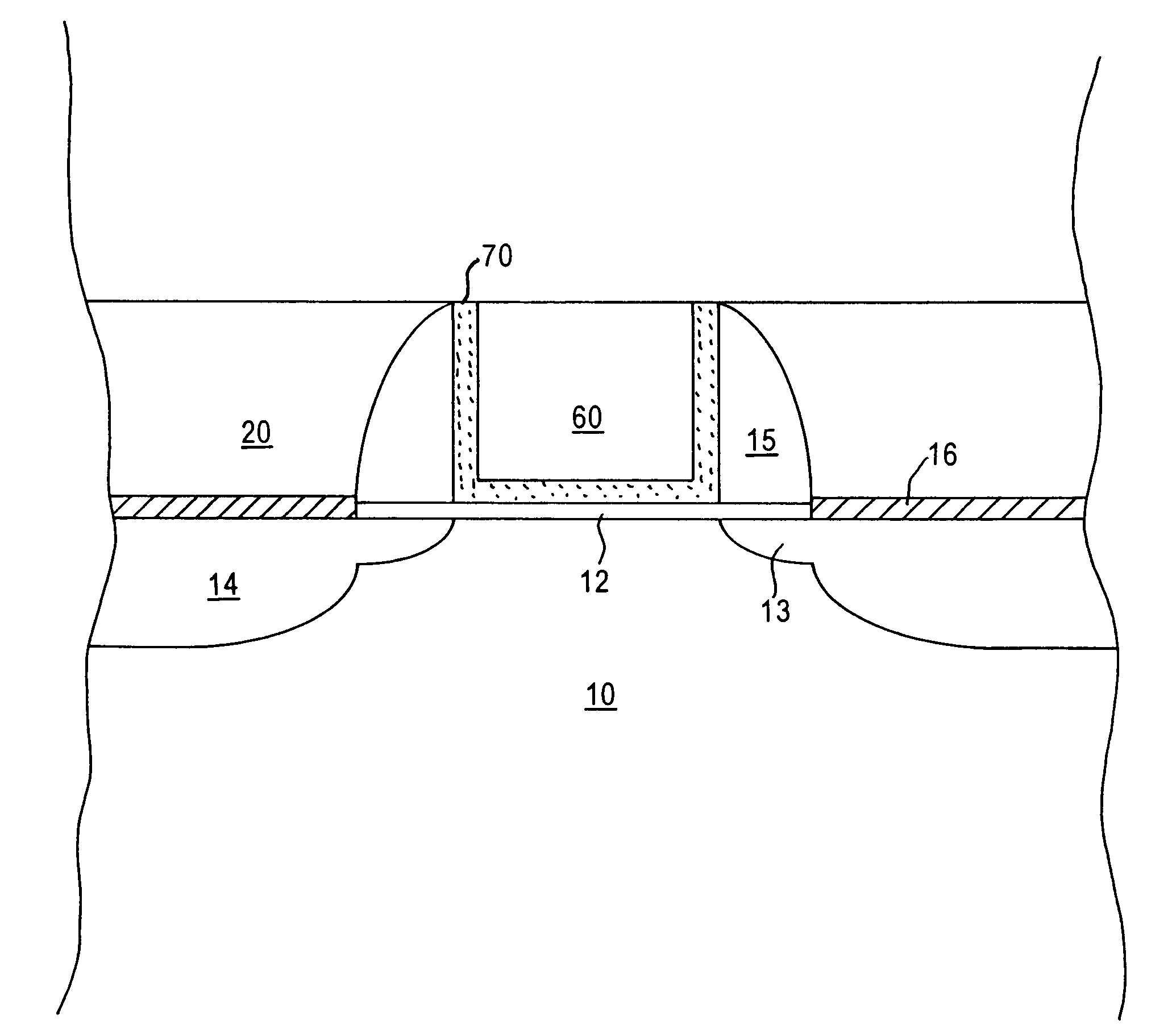
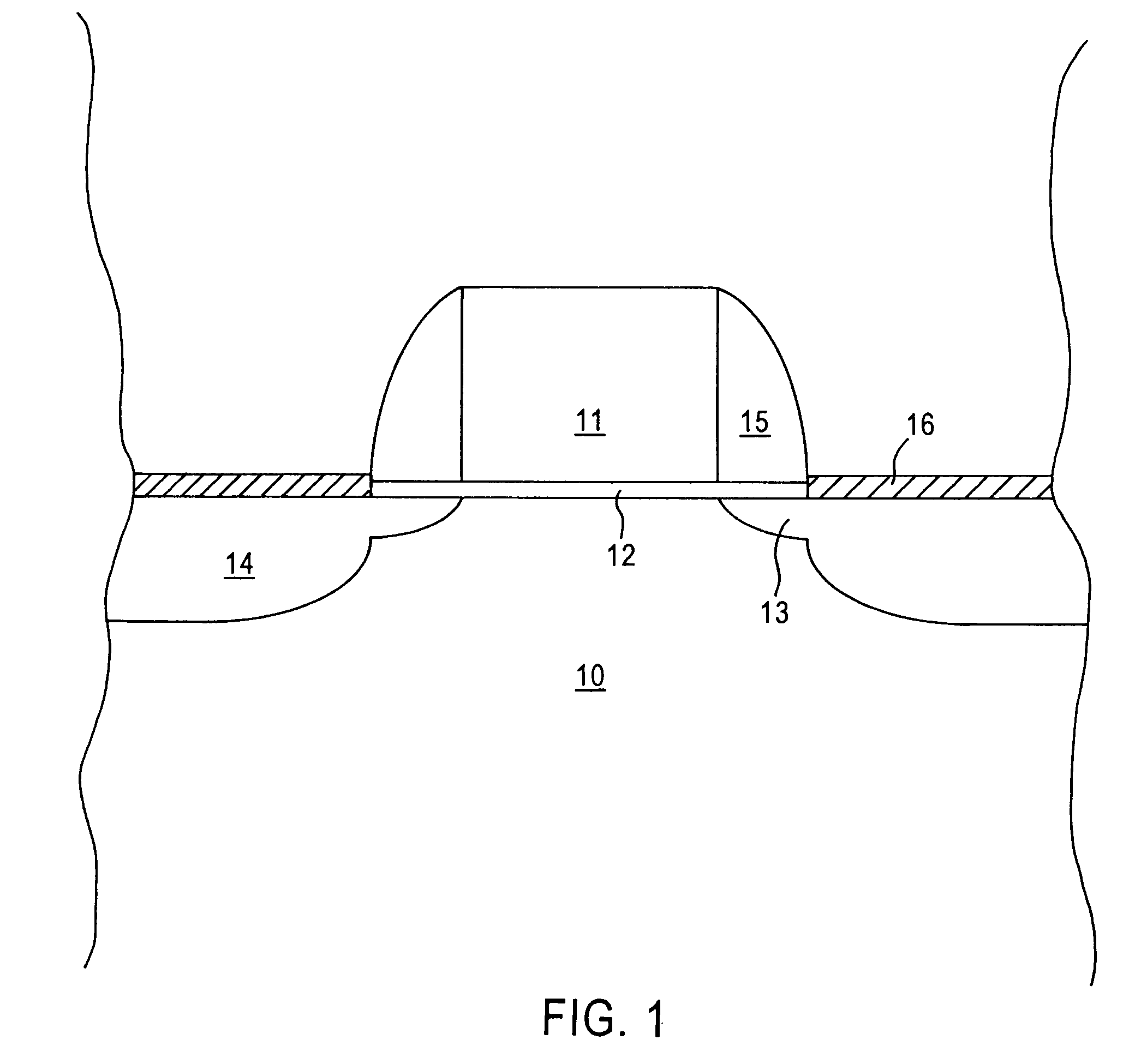
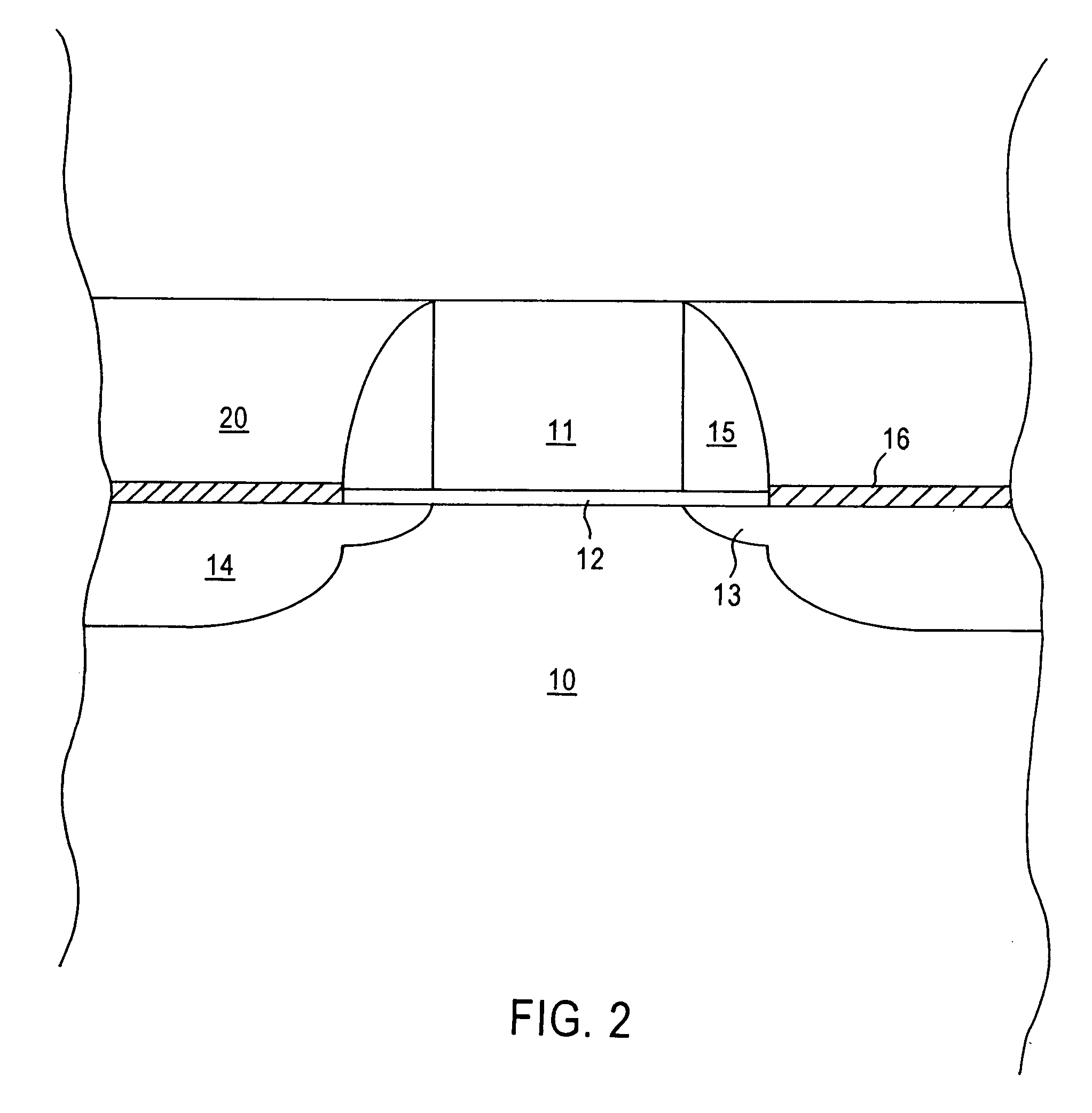
[0020]The present invention address and solves problems attendant upon conventional practices relating to the formation of polysilicon gate electrodes, which problems stem from their high resistivity and, hence, slower operating speed. The present invention also addresses and solves problems attendant upon attempting to reduce the gate oxide thickness of replacement metal gate transistors, such as increased leakage current and reduced operating speed.

[0021]The present invention addresses and solves such problems by providing metal gate transistors with gate oxides having a reduced EOT without an increase in leakage, e.g., gate oxides having a thickness of less than 15 Å, such as a thickness of 5 Å to 12 Å, e.g., 10 Å, by techniques which include forming a protective layer on the gate oxide layer, which protective layer has a graded composition between the gate oxide layer and the gate electrode layer. The formation of a graded protective layer reduces stress between the gate electro...


PUM

PropertyMeasurementUnit
dielectric constantaaaaaaaaaa
temperatureaaaaaaaaaa

Abstract

Thin effective gate oxide thickness with reduced leakage for replacement metal gate transistors is achieved by forming a protective layer between the gate oxide layer and metal gate electrode, thereby reducing stress. Embodiments include forming a protective layer of amorphous carbon containing metal carbides decreasing in concentration from the metal gate electrode toward the gate oxide layer across the protective layer. Embodiments of methodology include removing the removable gate, depositing a layer of amorphous carbon on the gate oxide layer, forming the metal gate electrode and then heating at an elevated temperature to diffuse metal from the metal gate electrode into the amorphous carbon layer, thereby forming the metal carbides. Embodiments also include metal gate transistors with a gate oxide layer having a high dielectric constant and silicon concentrated at the interfaces with the metal gate electrode and substrate.

Description

TECHNICAL FIELD[0001]The present invention relates to semiconductor devices comprising transistors with metal gate electrodes and reduced gate oxide leakage. The present invention is particularly applicable to high speed semiconductor devices having submicron design features.BACKGROUND ART[0002]The integration of hundreds of millions of circuit elements, such as transistors, on a single integrated circuit necessitates further dramatic scaling down or micro-miniaturization of the physical dimensions of circuit elements, including interconnection structures. Micro-miniaturization has engendered a dramatic increase in transistor engineering complexity, such as the inclusion of graded well-doping, epitaxial wafers, halo implants, tip implants, lightly doped drain structures, multiple implants for source / drain regions, silicidation of gates and source / drains, and multiple sidewall spacers, for example.[0003]The drive for high performance requires high speed operation of microelectronic c...

Claims


Application Information

Patent Timeline
Patent Type & Authority Patents(United States)
IPC IPC(8): H01L21/02
CPCH01L21/28088H01L21/28238H01L29/495H01L29/4966H01L29/513H01L29/517H01L29/66545H01L21/28008H01L29/78609
Inventor PAN, JAMESPELLERIN, JOHN
Owner ADVANCED MICRO DEVICES INC
Why Eureka
Try Eureka