Variable resistive element, manufacturing method for same, and non-volatile semiconductor memory device

a technology of resistive elements and manufacturing methods, applied in semiconductor devices, digital storage, instruments, etc., can solve the problems of difficulty in restricting inconsistencies and large power requirements for switching to a high resistance state, and achieve low power consumption, low resistance inconsistency, and high speed

Active Publication Date: 2011-11-08
SHARP KK +1
View PDF13 Cites 113 Cited by
  • Summary
  • Abstract
  • Description
  • Claims
  • Application Information

AI Technical Summary

Benefits of technology

[0013]A resistance change memory made of a binary transition metal oxide, as disclosed in Patent Document 2 and Non-Patent Document 2, has a high affinity with semiconductor processes and a simple structure and composition as described above, and has an advantage in that it can be easily applied for a non-volatile memory having high integration. On the other hand, the resistance change memory has problems with switching properties such that a rate of switching from a low resistance state to a high resistance state is low (not less than approximately μsec), and in addition, a current required for the switching is large (not less than approximately mA), and as a result, the power required for switching to a high resistance state is large.

Problems solved by technology

On the other hand, the resistance change memory has problems with switching properties such that a rate of switching from a low resistance state to a high resistance state is low (not less than approximately μsec), and in addition, a current required for the switching is large (not less than approximately mA), and as a result, the power required for switching to a high resistance state is large.
The element has a structure which makes a high speed operation possible, and it is expected that the difficulty in restricting inconsistencies at the microscopic level between elements will become a problem with implementing a memory having high integration, in particular, when the size of the elements become close to the size of the microscopic holes which are filled in with a metal.

Method used


Image

  • Variable resistive element, manufacturing method for same, and non-volatile semiconductor memory device
  • Variable resistive element, manufacturing method for same, and non-volatile semiconductor memory device
  • Variable resistive element, manufacturing method for same, and non-volatile semiconductor memory device

Examples


first embodiment

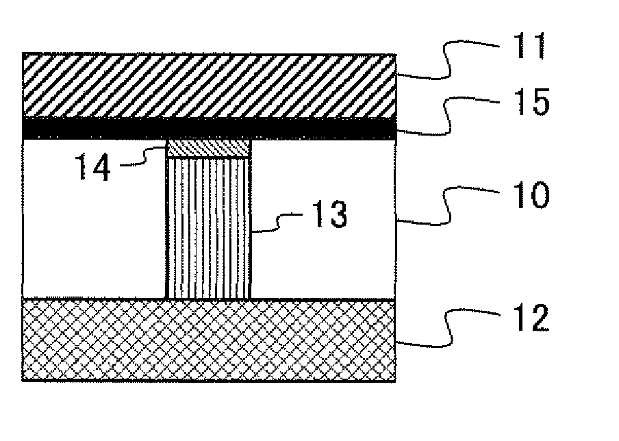
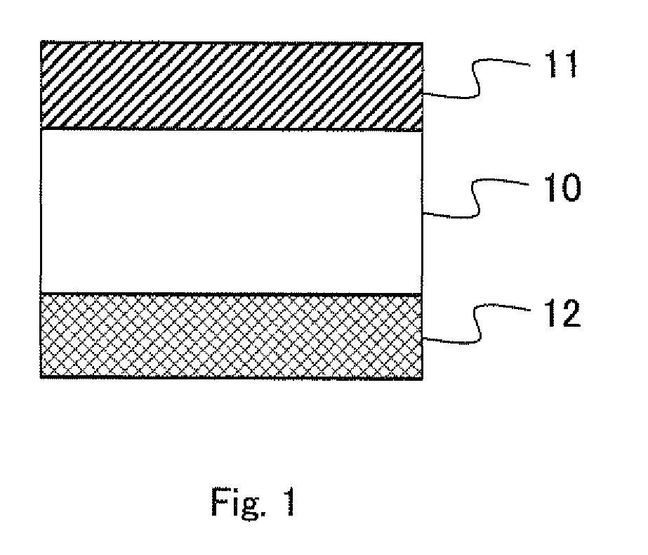
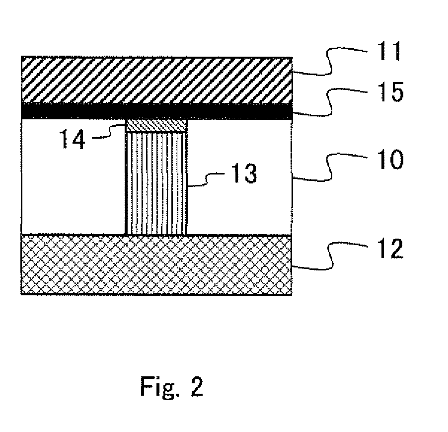
[0127]An element and a method according to a first embodiment of the present invention are described below with reference to FIGS. 1 to 24. The variable resistive element according to the present invention is a variable resistive element having an original structure with a metal oxide layer 10 between a first electrode 11 and a second electrode 12 as an element structure, as shown in FIG. 1, and an electrical resistance between the first and second electrodes 11 and 12 changes in a reversible manner in accordance with application of electrical stress across the first and second electrodes 11 and 12. In addition, in this variable resistive element, a filament 13, which is a current path where a density of a current flowing between the first and second electrodes 11 and 12 is locally high, is formed in the metal oxide layer 10 in a “forming” process described below, and part or the entirety of the filament 13 in FIG. 2 is connected or disconnected through a switching operation describ...

example 1

[0149]The original structure of the element according to the present invention was prototyped by forming films on a silicon substrate with a thermally oxidized film in the order of Ti / Pt (second electrode) / cobalt oxide (metal oxide layer) / Ta (first electrode) / Pt in the above-described mode. In addition, a first forming voltage of +9.9 V was applied to the first electrode with reference to the second electrode, and a second forming process for generating an interface oxide was carried out through heat treatment of 200° C. FIG. 8 shows a TEM photograph showing the element according to the present invention after the second forming process in a cross section. It can be seen that an interface oxide (tantalum oxide) having a thickness of approximately 5 nm was generated in the interface between the Ta electrode (first electrode) and the cobalt oxide (metal oxide layer). FIG. 9 shows the voltage pulse response (switching properties) of this element according to the present invention. It c...

example 2

[0150]The original structure of the element according to the present invention was prototyped by forming films on a silicon substrate with a thermally oxidized film in the order of Ti / Pt (second electrode) / cobalt oxide (metal oxide layer) / Ta (first electrode) / Pt in the above-described mode. FIG. 10 shows the IV properties of this element according to the present invention when a voltage is applied across the first and second electrodes. As shown by the arrows in FIG. 10, voltages were applied in the order of A, B, C and D. The voltage application indicated by A is a first forming process where the metal oxide layer is broken down through the application of a voltage of +10 V so that a filament is formed in a temporary low resistance state. The voltage application indicated by B is a second forming process where a large current flows in accordance with the resistance value of the filament in a low resistance state, and the Joule heat oxidizes the Ta electrode and the filament end in ...


PUM


Abstract

Provided is a variable resistive element which performs high speed and low power consumption operation. The variable resistive element comprises a metal oxide layer between first and second electrodes wherein electrical resistance between the first and second electrodes reversibly changes in accordance with application of electrical stress across the first and second electrodes. The metal oxide layer has a filament, which is a current path where the density of a current flowing between the first and second electrodes locally increases. A portion including at least the vicinity of an interface between the certain electrode, which is one or both of the first and second electrodes, and the filament, on an interface between the certain electrode and the metal oxide layer is provided with an interface oxide which is an oxide of at least one element included in the certain electrode and different from the oxide of the metal oxide layer.

Description

CROSS-REFERENCE TO RELATED APPLICATIONS[0001]This application is a National Phase filing under 35 U.S.C. §371 of International Application No. PCT / JP2008 / 056859 filed on Apr. 7, 2008, and which claims priority to Japanese Patent Applications No. 2007-126016 filed on May 10, 2007 and No. 2007-292763 filed on Nov. 12, 2007.TECHNICAL FIELD[0002]The present invention relates to a variable resistive element which can store information when an electrical resistance changes in accordance with application of an electrical stress, a manufacturing method for the same, and a non-volatile semiconductor memory device. In particular, the present invention relates to a variable resistive element which can perform high speed and low power consumption operation without reversible variable resistive properties of a metal oxide being damaged as a result of combination of a metal oxide material and an electrode material, a manufacturing method for the same, and a non-volatile semiconductor memory devic...

Claims


Application Information

Patent Timeline
Patent Type & Authority Patents(United States)
IPC IPC(8): G11C11/00
CPCG11C11/5614G11C11/5685G11C13/0007G11C13/0011G11C13/0069H01L27/101H01L45/08H01L45/1233H01L45/146G11C2013/0073G11C2013/0083G11C2013/009G11C2213/32G11C2213/34G11C2213/51G11C2213/56G11C2213/77H10N70/24H10N70/826H10N70/8833
Inventor TAMAI, YUKIOHOSOI, YASUNARIAWAYA, NOBUYOSHIOHNISHI, SHIGEOISHIHARA, KAZUYASHIMA, HISASHIAKINAGA, HIROYUKITAKANO, FUMIYOSHI
Owner SHARP KK
Why Eureka
Try Eureka