Organic semiconductor element with shield layer
a shield layer and organic semiconductor technology, applied in the direction of discharge tube luminescnet screen, discharge tube/lamp details, transportation and packaging, etc., can solve the problems of easy deterioration, short service life of elements, and inducing deterioration of organic materials, so as to suppress the deterioration of organic semiconductor elements and prolong the service life. , the effect of high efficiency
- Summary
- Abstract
- Description
- Claims
- Application Information
AI Technical Summary
Benefits of technology
Problems solved by technology
Method used
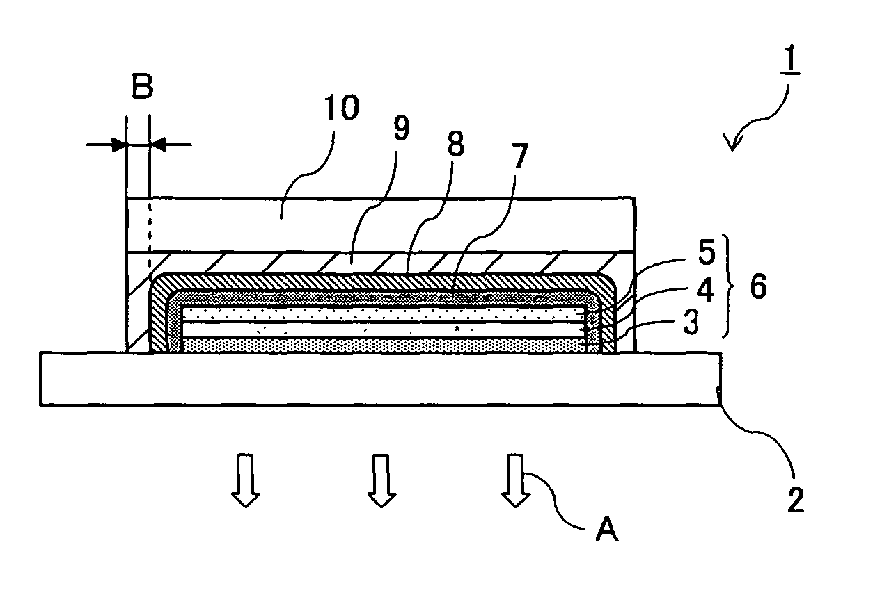
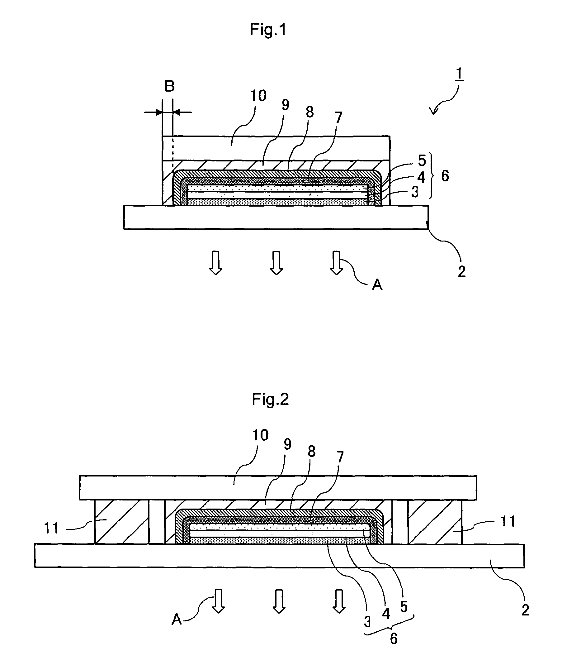
Image

Examples
experiment 1
[0060
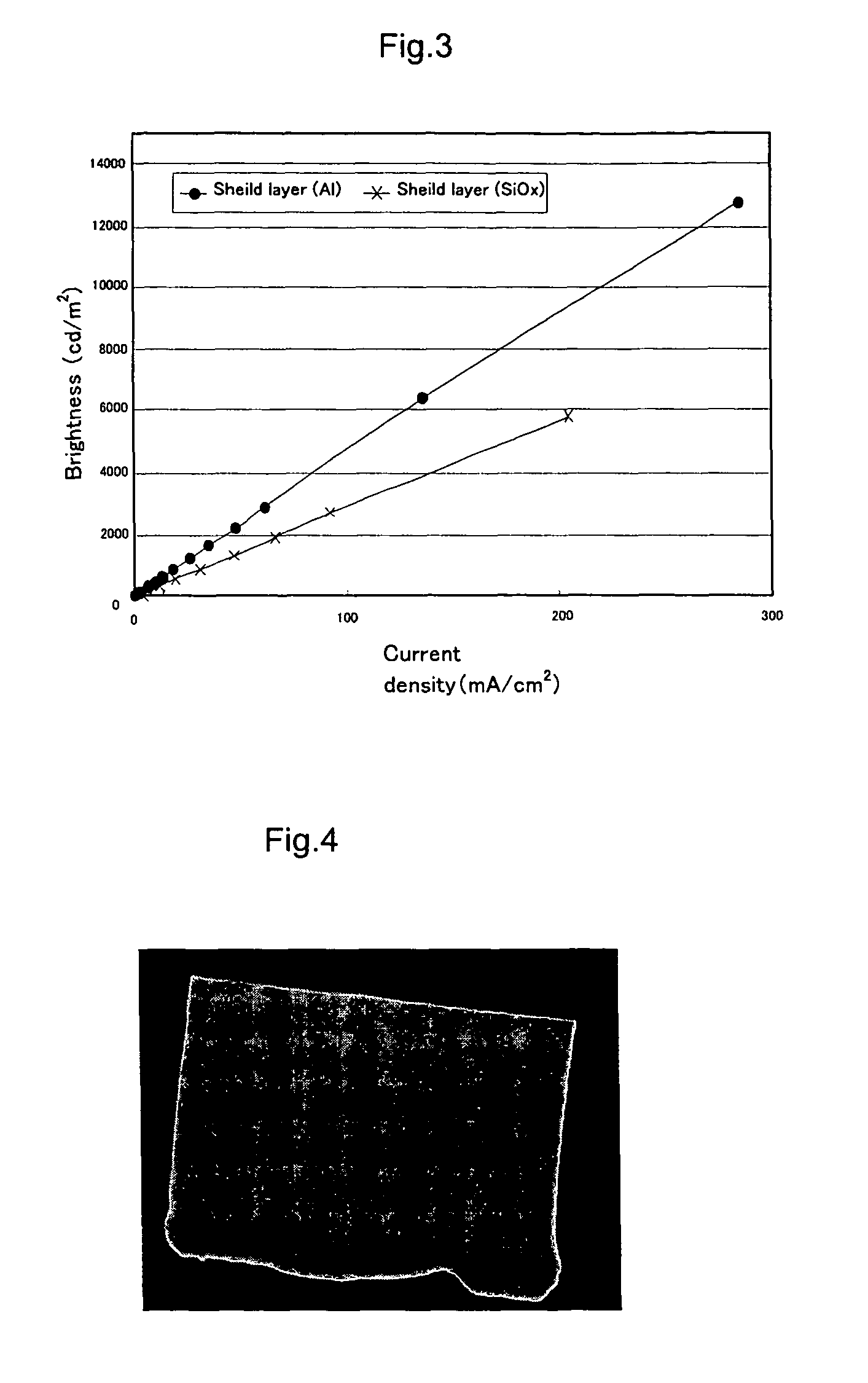
[0061]In this experiment, the influence of a shield layer on an organic EL element using a UV-curing resin for an adhesive layer was studied. First, CuPc (200 Å in thickness), α-NPD (200 Å in thickness), Alq (500 Å in thickness), LiF (10 Å in thickness), and Al (2000 Å in thickness) were vacuum deposited sequentially in the order mentioned by the resistance heating method on a cleaned ITO-applied glass substrate (0.7 mm in thickness) to form an organic layer and a cathode. Subsequently, polymonochloroparaxylylene (2 μm in thickness) was deposited as a planarizing layer by the hot CVD method and Al (6000 Å in thickness) was vacuum deposited as a shield layer by the resistance heating method. Then, a UV-curing epoxy resin was spread, a glass sheet (0.7 mm in thickness) was mounted as a radiator plate on the spread resin, and the resin was cured to produce the organic EL element. Incidentally, the UV-curing epoxy resin was cured with a metal halide lamp by radiating the UV light o...
experiment 2
[0063
[0064]In this experiment, the effect of a shield layer manifested when a thermosetting acrylic resin was used for an adhesive layer was studied. First, CuPc (200 Å in thickness), α-NPD (200 Å in thickness), Alq (500 Å in thickness), LiF (10 Å in thickness), and Al (2000 Å in thickness) were vacuum deposited sequentially in the order mentioned by the resistance heating method on a cleaned ITO-applied glass substrate (0.7 mm in thickness) to form an organic layer and a cathode. Subsequently, polymonochloroparaxylylene (2 μm in thickness) was deposited as a planarizing layer by the hot CVD method and Al (3 μm in thickness) was vacuum deposited as a shield layer by the resistance heating method. Then, a thermosetting acrylic resin was spread, a glass sheet (0.7 mm in thickness) was mounted as a radiator plate on the spread resin, and the resin was cured under the conditions of 90° C. in temperature and one hour in period to produce the organic EL element. The device size (light-emi...
experiment 3
[0066
[0067]In this experiment, the positional relation between the radiator plate and the element. First, CuPc (200 Å in thickness), α-NPD (200 Å in thickness), Alq (500 Å in thickness), LiF (10 Å in thickness), and Al (2000 Å in thickness) were vacuum deposited sequentially in the order mentioned by the resistance heating method on a cleaned ITO-applied glass substrate (0.7 mm in thickness) to form an organic layer and a cathode. Subsequently, polymonochloroparaxylylene (2 μm in thickness) was deposited as a planarizing layer by the hot CVD method and Al (3000 Å in thickness) was vacuum deposited as a shield layer by the resistance heating method. Then, a UV-curing epoxy resin was spread, a glass sheet (0.7 mm in thickness) was mounted as a radiator plate on the spread resin, and the resin was cured to produce the organic EL element. Incidentally, the UV-curing epoxy resin was cured with a metal halide lamp by radiating the UV light of a wavelength of 365 nm contained in the lamp a...
PUM
 Abstract
Description
Claims
Application Information
 - R&D
- Intellectual Property
- Life Sciences
- Materials
- Tech Scout
- Unparalleled Data Quality
- Higher Quality Content
- 60% Fewer Hallucinations
Browse by: Latest US Patents, China's latest patents, Technical Efficacy Thesaurus, Application Domain, Technology Topic, Popular Technical Reports.
© 2025 PatSnap. All rights reserved.Legal|Privacy policy|Modern Slavery Act Transparency Statement|Sitemap|About US| Contact US: help@patsnap.com