Differential-to-single ended signal converter circuit and method

Active Publication Date: 2011-12-27
MONTEREY RES LLC
View PDF1125 Cites 18 Cited by
  • Summary
  • Abstract
  • Description
  • Claims
  • Application Information

AI Technical Summary

Problems solved by technology

In addition, such signals may not exhibit sufficient differential voltage to fully switch output states (high, low) of a conventional differential to single ended signal converter.
Conventional differential to single ended solutions that rely on differential sensing may not be suitable for use with latched differential signals like those described above.
In particular, as noted above,

Method used


Image

  • Differential-to-single ended signal converter circuit and method
  • Differential-to-single ended signal converter circuit and method
  • Differential-to-single ended signal converter circuit and method

Examples


first embodiment

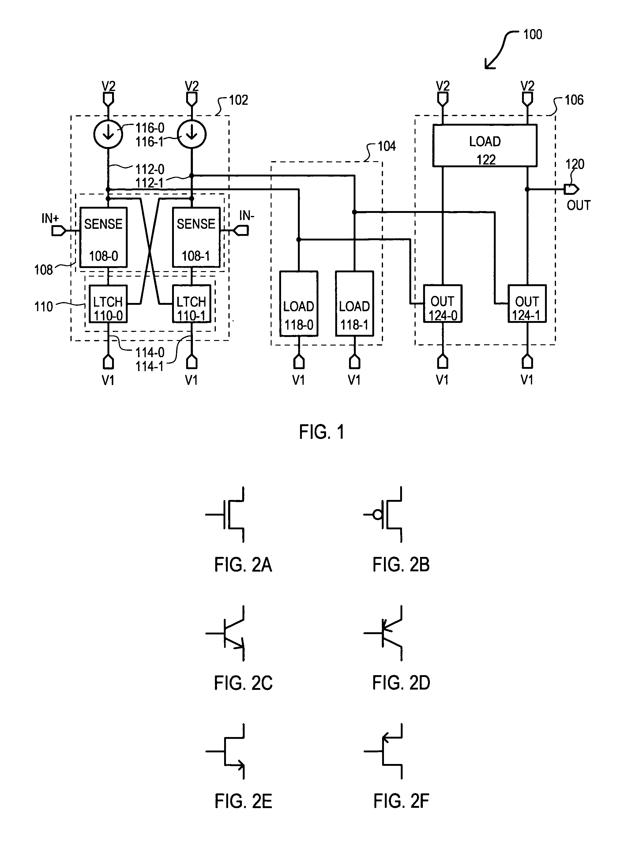
[0026]A differential to single ended conversion circuit is shown in block schematic diagram in FIG. 1, and designated by the general reference character 100. A circuit 100 can receive an input that includes a first differential input signal IN+ and a second differential input signal IN−, and can provide a single ended output signal OUT.

[0027]A circuit 100 can include an input section 102, a load section 104, and an output section 106. An input section 102 can latch opposite states based on differential input signals.

[0028]In the particular example of FIG. 1, an input section 102 can include a differential sense section 108 and a latching section 110. A differential sense section 108 can include a first sense device 108-0 and a second sense device 108-1. Sense devices (108-0 and 108-1) can be active device, such as transistors, that can provide a controllable impedance path (e.g., source-drain, collector-emitter) according to a control terminal (e.g., gate or base). Sense device 108...

second embodiment

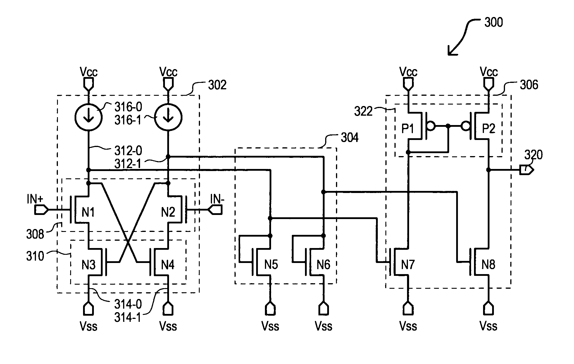
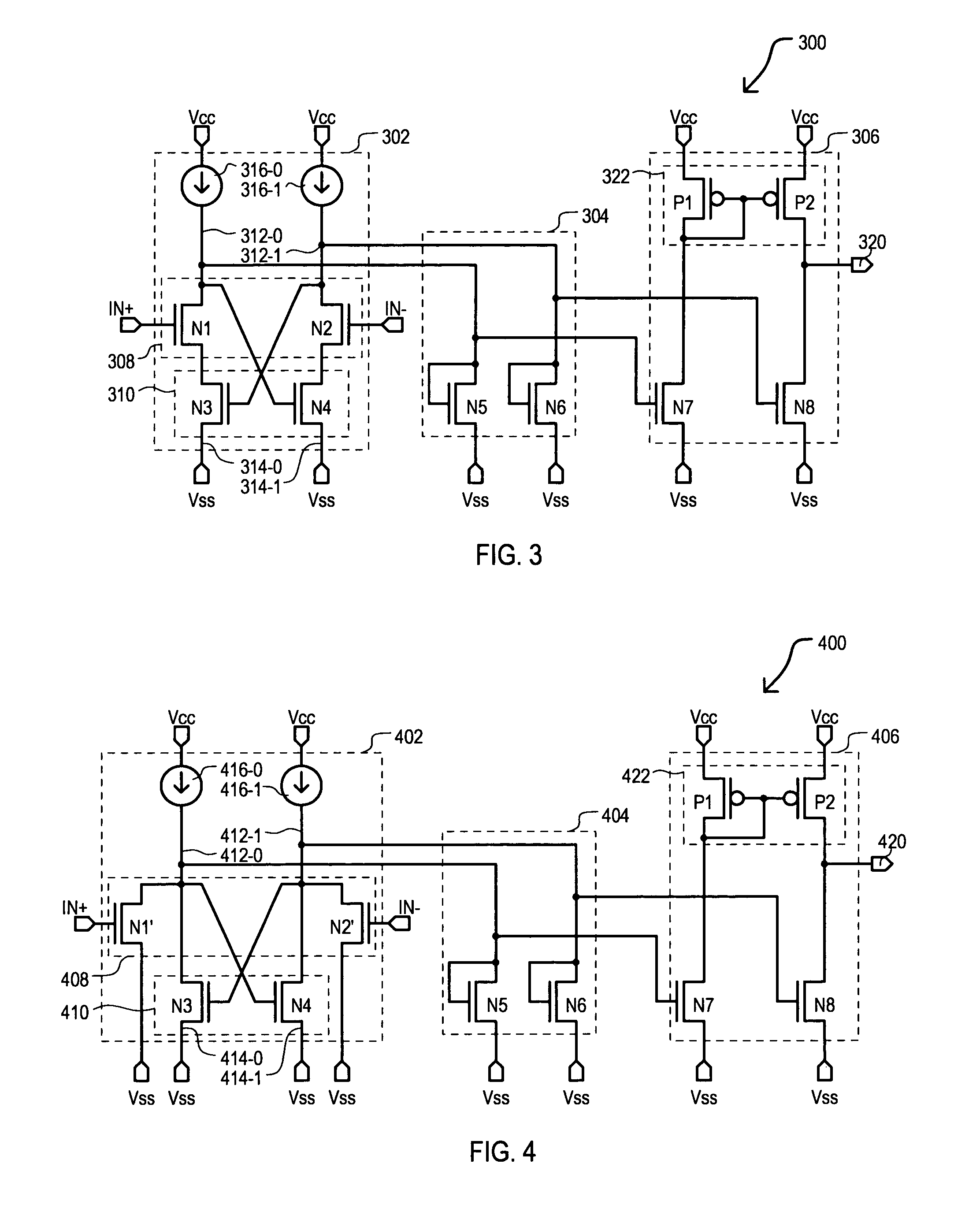
[0041]Referring now to FIG. 3, a latched differential-to-single ended signal converter circuit is shown in schematic diagram, and designated by the general reference character 300. A circuit 300 can include some of the same general sections as FIG. 1, thus like sections are referred to by the same reference character, but with the first digit being a “3” instead of a “1”.

[0042]FIG. 3 shows an arrangement in that can receive a potentially problematic latched differential signal (differential signals whose crossing point is very close to a maximum signal voltage) and convert it into a single-ended full swing logic signal with nearly the same duty cycle as the differential signal. That is, when latched differential signals having crossing points with essentially 50% duty cycles, a circuit 300 can provide a resulting output signal with a corresponding 50% duty cycle.

[0043]The circuit 300FIG. 3 shows an example of a “NAND” type arrangement. An input section 302 can include a differentia...

fifth embodiment

[0060]Referring now to FIG. 6, a phase locked loop (PLL) circuit is shown in a block schematic diagram and designated by the general reference character 600. A PLL 600 can include a phase detector 602, a filter section 604, a voltage controlled oscillator (VCO) 606, an output stage 608, and a feedback path 610. A phase detector 602 can receive an input signal Sin and a feedback signal Sfdbk, and determine a phase difference between such values ph_diff. A phase difference value ph_diff can be filtered by a filter section to generate a control voltage Ve. A VCO 606 can be a ring oscillator that generates a differential signal IN+ / IN− whose output frequency can vary according to control voltage Ve. As but one example, a VCO can be a ring oscillator signal like that shown as 500 in FIG. 5.

[0061]Referring still to FIG. 6, output stage 608 can receive differential input signals IN+ / IN−, and in response thereto, generate a single ended output signal Sout. An output stage 608, like that sh...


PUM


Abstract

A differential-to-single ended converter circuit can include a latching circuit having first and second latch field effect transistors (FETs) with drains and gates cross-coupled between a first latch node and a second latch node. The source-drain paths of the first and second latch FETs are coupled to a first reference potential node via separate current paths. A sense circuit can include a first sense FET having a source-drain path coupled between the first sense node and the first reference potential node, and a gate coupled to a first input node. A second sense FET has a source-drain path coupled between the second sense node and the first reference potential node, and a gate coupled to a second input node. An output circuit can have a first output FET with a source-drain path coupled between a first output supply node and an output signal node, and a gate coupled to the first latch node, and a second output FET with a source-drain path coupled between the output signal node and a second output supply node.

Description

[0001]This application claims the benefit of U.S. provisional application Ser. No. 60 / 752,804 filed Dec. 21, 2005, the contents of which are incorporated by reference herein.TECHNICAL FIELD[0002]The present invention relates generally to electronic circuits, and more particularly to signal converter circuits that can convert one or more received input signals into one or more output signals of a different convention type than the input signal(s).BACKGROUND OF THE INVENTION[0003]A signal converter circuit can convert input signals having a particular convention (e.g., shape, amplitude, number of phases, and / or offset) for use by other circuits that require a different signal convention. One type of conversion can be from two differential input signals into one single swing output signal.[0004]To better understand various features of the disclosed embodiments, conventional approaches to converting differential input signals into a single ended output signal will first be described.[00...

Claims


Application Information

Patent Timeline
IPC IPC(8): G11C7/06
CPCH03F3/45179H03F2203/45318
Inventor STIFF, JONATHON
Owner MONTEREY RES LLC
Why Eureka
Try Eureka