Thermal method to control underfill flow in semiconductor devices

a semiconductor device and underfill technology, applied in the field of electronic systems and semiconductor devices, can solve the problems of shrinkage of the bump center-to-center pitch, insufficient approaches, and event-driven assembly failure, and achieve the effects of simple and low-cost assembly process, high number and small bump siz

Active Publication Date: 2012-02-07
TEXAS INSTR INC
View PDF4 Cites 1 Cited by
  • Summary
  • Abstract
  • Description
  • Claims
  • Application Information

AI Technical Summary

Benefits of technology

[0009]It is a technical advantage of the invention that the assembly process is simple and low-cost, applicable to large-chip semiconductor products, high numbers and small size of bumps, and fine bump pitch. At the same time, the method is flexible and can be applied to a wide spectrum of material and process variations, leading to improved semiconductor device reliability.

Problems solved by technology

These stresses tend to fatigue the solder bump interconnections, resulting in cracks and thus eventual failure of the assembly.
These approaches become increasingly insufficient as the number of bump interconnections increases and the bump size and the bump center-to-center pitch shrink.
With these trends, the number of voids in the underfill and the risk of clustering the fillers in the precursor increase sharply.

Method used


Image

  • Thermal method to control underfill flow in semiconductor devices
  • Thermal method to control underfill flow in semiconductor devices
  • Thermal method to control underfill flow in semiconductor devices

Examples


Embodiment Construction

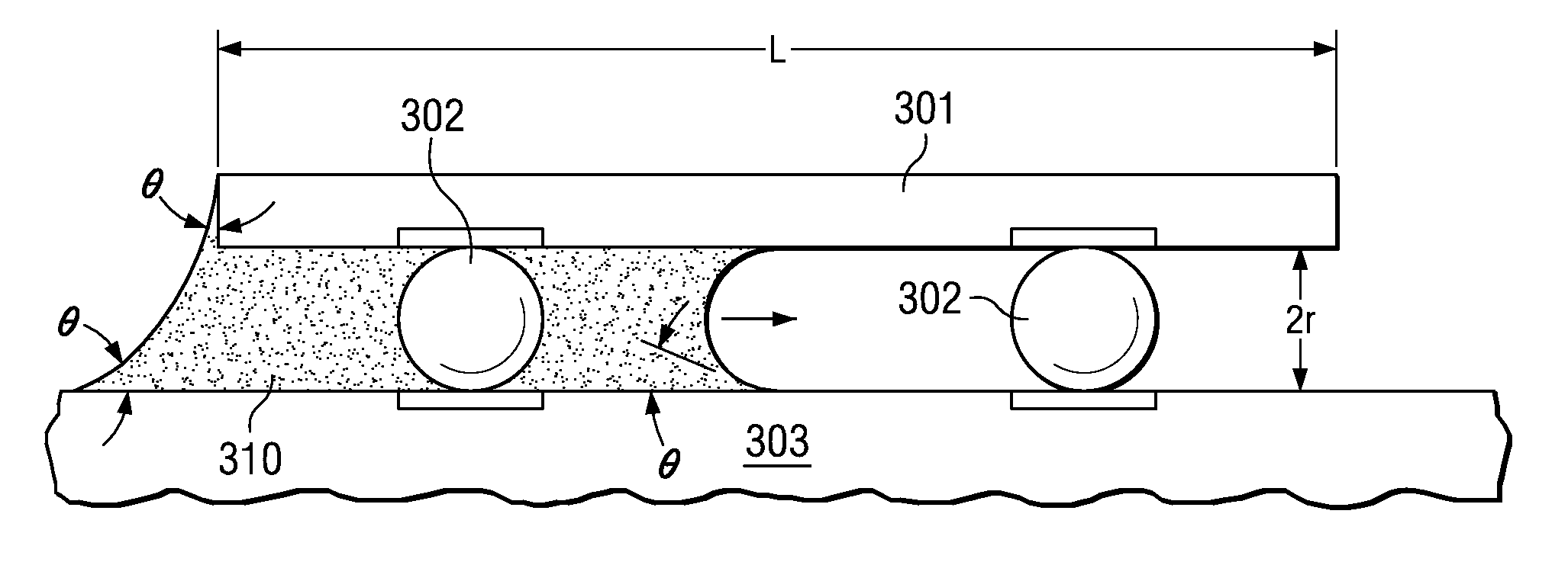
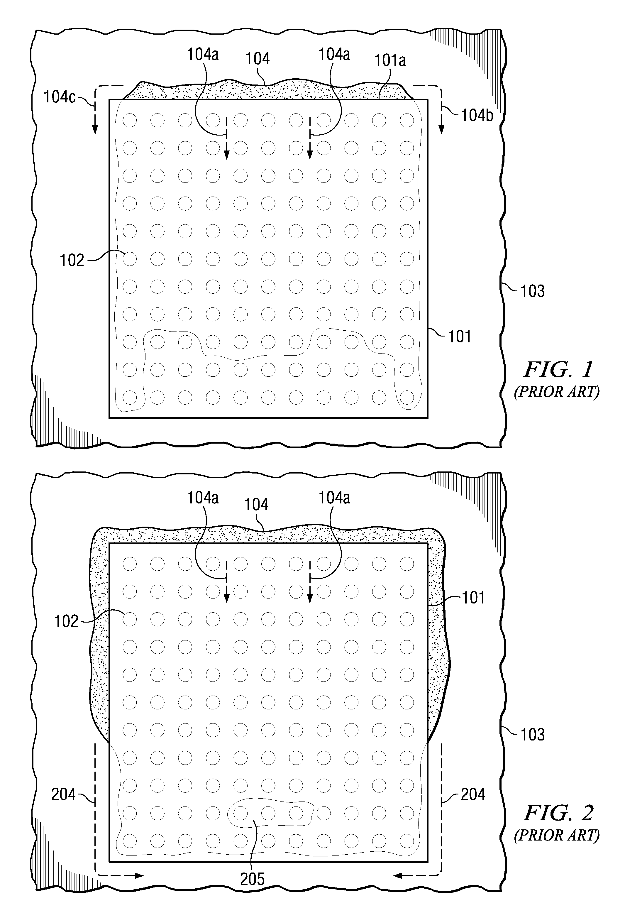
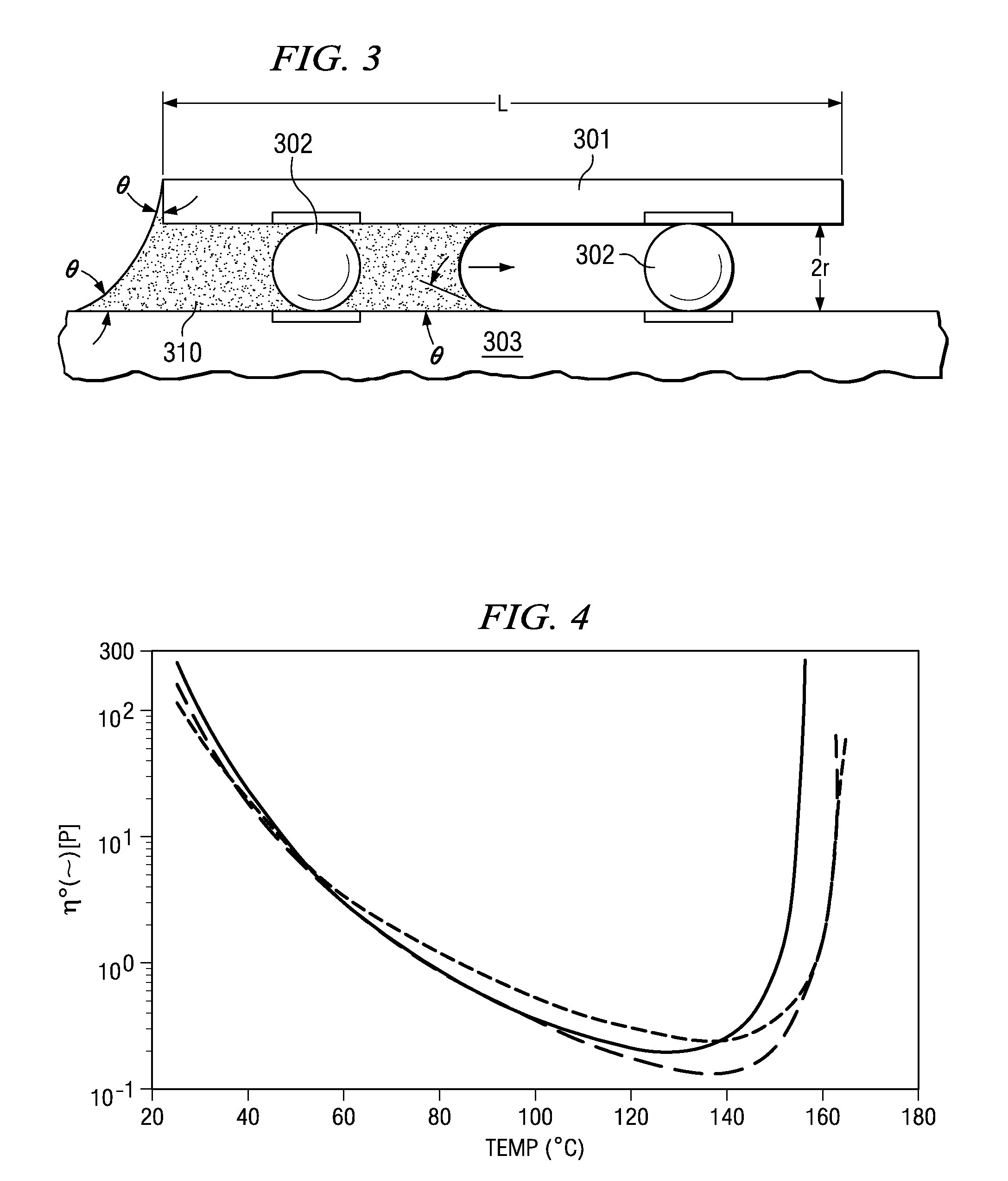
[0021]The schematic top X-ray views of FIGS. 1 and 2 illustrate a typical example of an underfill process in known technology of a semiconductor chip assembled on a substrate. Looking through the flip-assembled transparent chip 101, FIGS. 1 and 2 show rows of solder connections 102 connecting the chip and to the substrate 103 (also transparent). The solder connections 102 between chip 101 and substrate 103 create a gap. A quantity of liquid, viscous polymeric material 104 is deposited along chip side 101a for filling this gap; capillarity pulls the polymer into the gap and provides the mechanism for filling.

[0022]Capillarity is the capillary action by which the surface of a liquid, where it contacts a solid, is elevated or depressed, because of the relative attraction of the molecules of the liquid for each other and for those of the solid. Capillary attraction is the force of adhesion existing between a solid and a liquid in capillarity.

[0023]Capillary action becomes effective, whe...


PUM


Abstract

A method and apparatus for assembling a semiconductor device. A chip (901) with solder bodies (903) on its contact pads is flipped onto a substrate (904). After the reflow process, a gap (910) spaces chip and substrate apart. A polymer precursor is selected for its viscosity of known temperature dependence. The apparatus has a plate (800) with heating and cooling means to select and control a temperature profile from location to location across the plate. After preheating, the assembly is placed on a mesa (801) of the plate configured to heat only a portion of the substrate. Movable capillaries (840, 921) blow cooled gas onto selected locations of the assembly. After the temperature profile is reached, a quantity of the precursor is deposited at a chip side and pulled into the gap by capillary action. The capillary flow is controlled by controlling the precursor viscosity based on the temperature profile, resulting in a substantially linear front, until the gap is filled substantially without voids.

Description

FIELD OF THE INVENTION[0001]The present invention is related in general to the field of electronic systems and semiconductor devices and more specifically to structure and method of void-free underfilling the gap of flip-chip electronic assemblies.DESCRIPTION OF THE RELATED ART[0002]It is well known in the so-called flip-chip technology how to mount an integrated circuit chip to a substrate such as a printed circuit board by solder bump interconnections. After the assembly process, the integrated circuit chip is spaced apart from the printed circuit substrate by a gap. The solder bump interconnections extend across the gap and connect contact pads on the integrated circuit chip to terminal pads on the printed circuit substrate to attach the chip and then conduct electrical signals, power and ground potential to and from the chip for processing. Similarly, after packaged semiconductor devices of the ball grid array families have been assembled to motherboards by means of solder bumps...

Claims


Application Information

Patent Timeline
Patent Type & Authority Patents(United States)
IPC IPC(8): H01L21/44
CPCH01L21/563H01L24/28H01L2924/10253H01L2924/014H01L2924/01087H01L2224/73203H01L2224/83102H01L2224/92125H01L2924/01015H01L2924/0102H01L2924/01029H01L2924/01032H01L2924/01047H01L2924/0105H01L2924/01082H01L2924/14H01L2924/01006H01L2924/01023H01L2924/01033H01L2924/3512H01L2924/00H01L2924/15787
Inventor GUPTA, VIKASLIBRES, JEREMIAS PEREZGRIGALUNAS, JOSEPH EDWARD
Owner TEXAS INSTR INC
Why Eureka
Try Eureka