Grooved substrates for uniform underfilling solder ball assembled electronic devices

a technology of underfilling and grooved substrates, applied in semiconductor devices, semiconductor/solid-state device details, electrical apparatus, etc., can solve the problems of increasing insufficient approaches, shrinking of bump center-to-center pitch, and event-based assembly failure, and achieve simple and low-cost assembly process, high number and small bump size

Active Publication Date: 2006-03-09
TEXAS INSTR INC
View PDF8 Cites 11 Cited by
  • Summary
  • Abstract
  • Description
  • Claims
  • Application Information

AI Technical Summary

Benefits of technology

[0010] It is a technical advantage of the invention that the assembly process is simple and low-cost, applicable to large-chip semiconductor products, high numbers and small size of bumps, and fine bump pitch. At the same time, the method is flexible and can be applied to a wide spectrum of material and process variations, leading to improved semiconductor device reliability.
[0011] The technical advances represented by the invention, as well as the aspects thereof, will become apparent from the following description of the preferred embodiments of the invention, when considered in conjunction with the accompanying drawings and the novel features set forth in the appended claims.

Problems solved by technology

These stresses tend to fatigue the solder bump interconnections, resulting in cracks and thus eventual failure of the assembly.
These approaches become increasingly insufficient as the number of bump interconnections increases and the bump size and the bump center-to-center pitch shrink.
With these trends, the number of voids in the underfill and the risk of clustering the fillers in the precursor increase sharply.

Method used


Image

  • Grooved substrates for uniform underfilling solder ball assembled electronic devices
  • Grooved substrates for uniform underfilling solder ball assembled electronic devices
  • Grooved substrates for uniform underfilling solder ball assembled electronic devices

Examples


Embodiment Construction

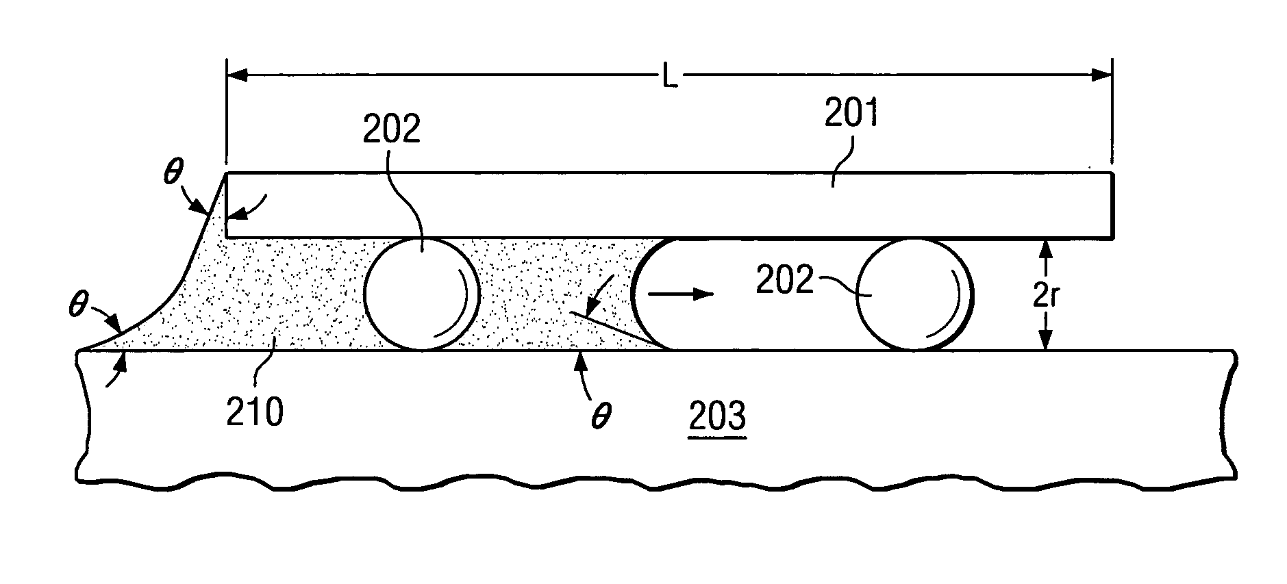
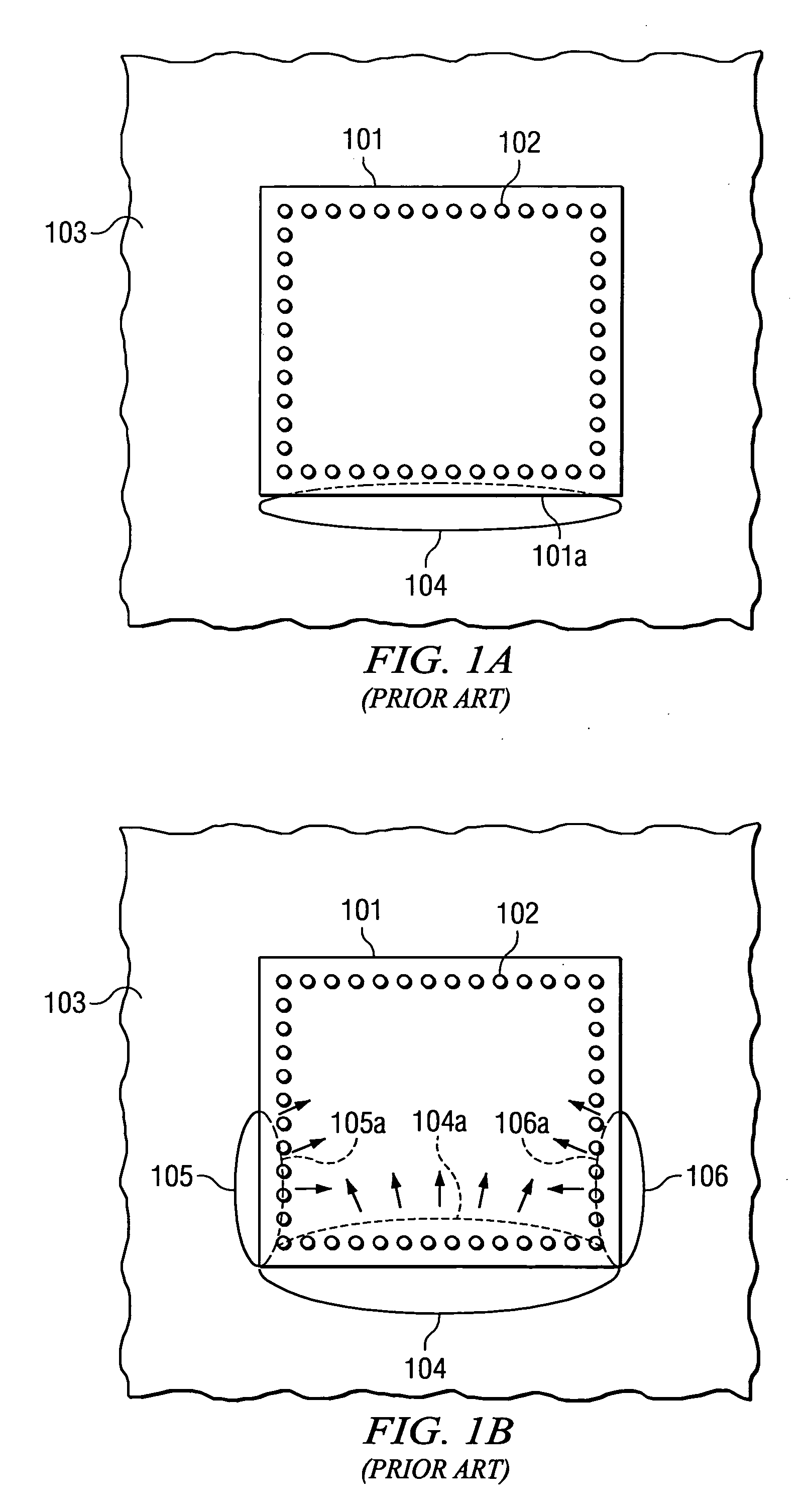
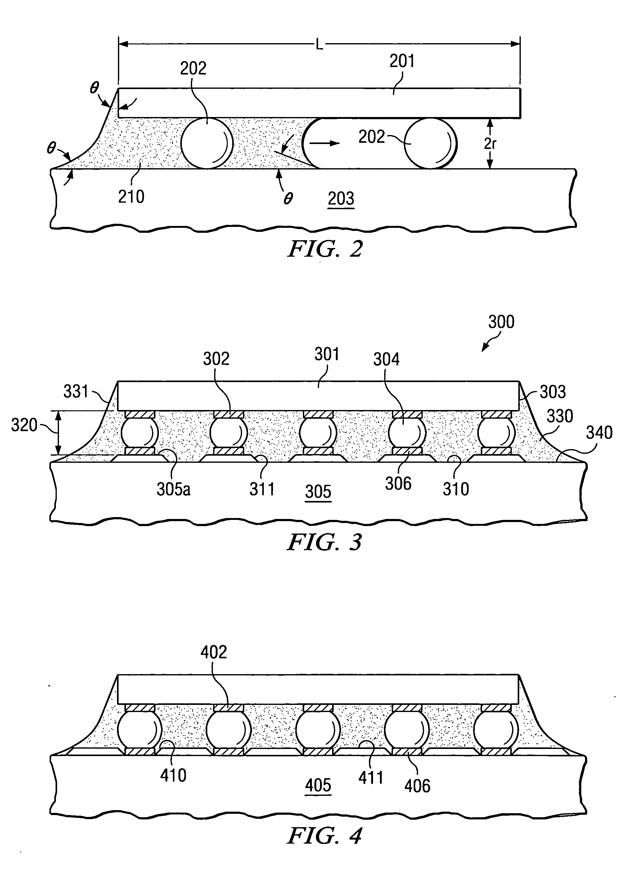
[0023] The impact of the present invention can be most easily appreciated by highlighting the shortcomings of the known technology. As a typical example of the known technology, the schematic top views of FIGS. 1A and 1B illustrate an assembly of a semiconductor chip 101 with rows of solder connections 102 around the chip perimeter onto a substrate 103. FIG. 1A shows in X-ray fashion the flip-assembled chip 101 attached to substrate 103; the solder connections 102 between chip 101 and substrate 103 create a gap. A quantity of liquid, viscous polymeric material 104 is deposited along chip side 101a for filling this gap; capillarity pulls the polymer into the gap and provides the mechanism for filling.

[0024] Capillarity is the capillary action by which the surface of a liquid, where it contacts a solid, is elevated or depressed, because of the relative attraction of the molecules of the liquid for each other and for those of the solid. Capillary attraction is the force of adhesion ex...


PUM


Abstract

A semiconductor assembly (300) comprising a semiconductor device (301), which has a plurality of metallic contact pads (302) and an outline by sides (303). A metallic bump (304) made of reflowable metal is attached to each of these contact pads. An electrically insulating substrate (305) has a surface with a plurality of metallic terminal pads (306) in locations matching the locations of the device contact pads, and further a plurality of grooves (310) and humps (311) distributed between the terminal pad locations, complementing the distribution of the terminal pads. Each bump is further attached to its matching terminal pad, respectively; the device is thus interconnected with the substrate and spaced apart by a gap (320). Adherent polymeric material (330) containing inorganic fillers fills the gap substantially without voids.

Description

FIELD OF THE INVENTION [0001] The present invention is related in general to the field of electronic systems and semiconductor devices and more specifically to structure and method of void-free underfilling the gap of flip-chip electronic assemblies. DESCRIPTION OF THE RELATED ART [0002] It is well known in the so-called flip-chip technology how to mount an integrated circuit chip to a printed circuit substrate by solder bump interconnections. After the assembly process, the integrated circuit chip is spaced apart from the printed circuit substrate by a gap. The solder bump interconnections extend across the gap and connect contact pads on the integrated circuit chip to terminal pads on the printed circuit substrate to attach the chip and then conduct electrical signals, power and ground potential to and from the chip for processing. Similarly, after packaged semiconductor devices of the ball grid array families have been assembled to motherboards by means of solder bumps connection...

Claims


Application Information

Patent Timeline
Patent Type & Authority Applications(United States)
IPC IPC(8): H01L21/50H01L21/44H01L23/48H01L23/28
CPCH01L21/563H01L24/28H01L2924/10253H01L2924/01087H01L2924/01023H01L2224/16225H01L2224/73203H01L2224/73204H01L2224/83102H01L2224/92125H01L2924/01005H01L2924/01015H01L2924/01033H01L2924/0105H01L2924/01052H01L2924/01079H01L2924/01082H01L2924/14H01L2924/19041H01L2924/01006H01L2924/3512H01L2924/00H01L2924/15787H01L2224/05573H01L2224/05568H01L2224/056H01L2924/00014H01L2224/0554H01L2224/05599H01L2224/0555H01L2224/0556
Inventor LIBRES, JEREMIAS P.MEDINA, JOEL T.MILLER, MARY C.
Owner TEXAS INSTR INC
Why Eureka
Try Eureka