Semiconductor integrated circuit for reducing crosstalk

a technology of integrated circuits and semiconductors, applied in the direction of voltage/current interference elimination, pulse technique, reliability increasing modifications, etc., can solve the problems of inability to settle crosstalk, more time in the design of the package, and crosstalk between the signal wires, so as to reduce the amount of crosstalk

Inactive Publication Date: 2012-02-14
KK TOSHIBA
View PDF4 Cites 6 Cited by
  • Summary
  • Abstract
  • Description
  • Claims
  • Application Information

AI Technical Summary

Benefits of technology

[0008]An aspect of the present invention provides a semiconductor integrated circuit for transmitting output signals based on a specific signal and two adjacent signals to a specific signal wire and two adjacent signal wires respectively, which includes an adjustment quantity calculation portion to calculate an adjustment quantity representing a degree of decrease of a slew rate of the specific signal, based on an adjustment coefficient for reducing an occurrence amount of crosstalk arising between the specific signal wire and the two adjacent signal wires and the specific signal and the two adjacent signals, and a driver to adjust the slew rate of the specific signal based on the adjustment quantity and to transmit one of the output signals corresponding to the specific signal.

Problems solved by technology

The signal transition may cause crosstalk between the signal wires.
The crosstalk is a signal interference occurring between the signal wires when the signal wires are arranged in physical proximity to each other.
However, these kinds of improvements may cause the following problems.
In the former improvement, package designing process needs to be repeated in order to increase noise margin, and accordingly, it takes more time in designing the package.
In addition, due to restriction of design, it may be impossible to settle the crosstalk.
Further, the cost of fabricating the package may increase.

Method used


Image

  • Semiconductor integrated circuit for reducing crosstalk
  • Semiconductor integrated circuit for reducing crosstalk
  • Semiconductor integrated circuit for reducing crosstalk

Examples


first embodiment

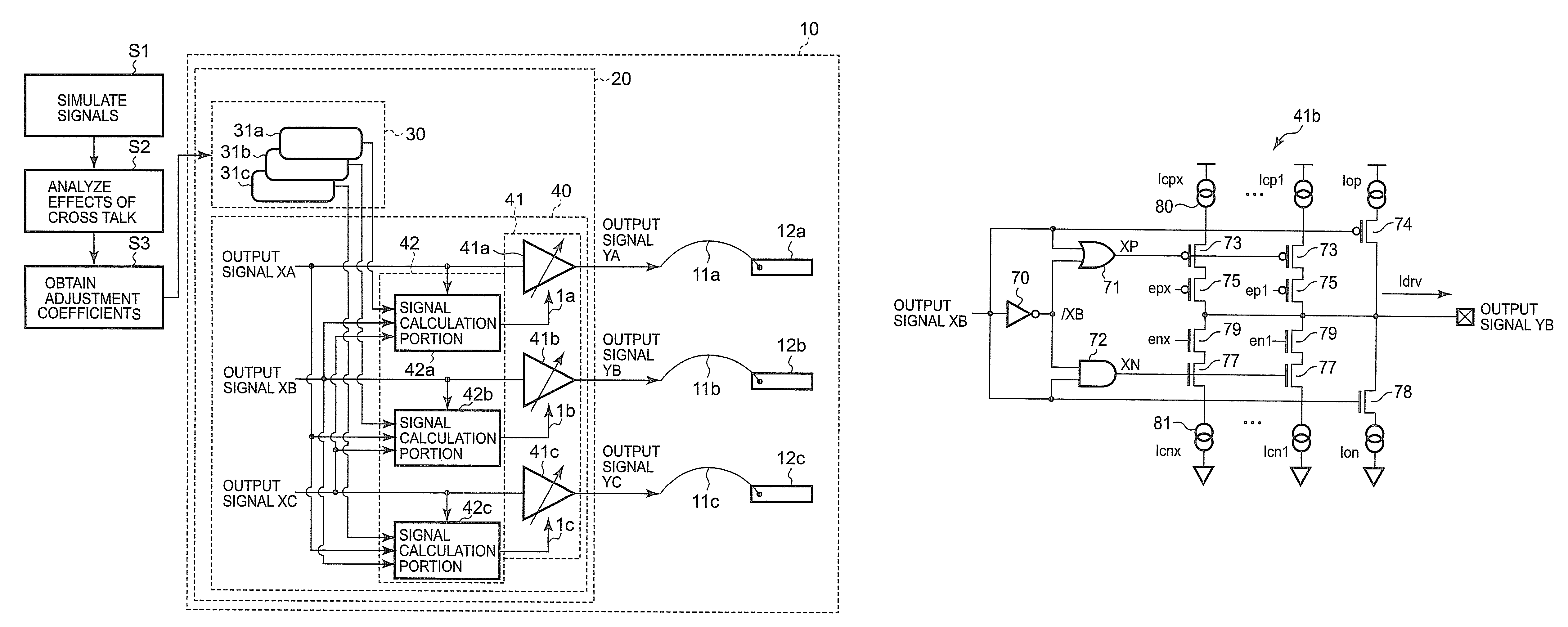
[0047]Subsequently, relationship between the adjustment quantity shown in FIG. 6 and the slew rate adjusted by the driver 41b of FIG. 4 will be explained with reference to FIGS. 7 and 8. FIG. 7 is a block diagram showing an internal configuration of a driver according to the invention. FIG. 8 is a figure showing a timing chart of the driver of FIG. 7.

[0048]First, the table of FIG. 6 shows, as an example, the adjustment quantity output by the calculation circuit 51 and the slew rate corresponding to the value of the adjustment quantity. The adjustment quantity is represented by a value such as 1, 2 or 3. For example, when the adjustment quantity is “1”, the slew rate is set to 25 psec. Likewise, the value of the adjustment quantity and the value of the slew rate correspond with each other such as follows. When the adjustment quantity=2, the slew rate is 50 psec. When the adjustment quantity=3, the slew rate is 75 psec.

[0049]The table of FIG. 6 shows current values Iop and Icp1-Icp3 o...

second embodiment

[0069]FIG. 9 is a block diagram showing a configuration of a semiconductor integrated circuit according to the invention.

[0070]In the second embodiment, adjustment coefficients 61a to 61c stored in an LSI external memory 60 are used to generate adjustment quantities. In this way, since the adjustment coefficients 61a to 61c are stored in the LSI external memory 60, the adjustment coefficient 61a to 61c may be copied from the LSI external memory 60 to the LSI internal memory 30 after the LSI 10 is installed. Then, the adjustment quantities can be generated.

[0071]As described above, the signal drive circuit according to the embodiment includes the signal calculation portions 42a to 42c that outputs the adjustment quantities using the adjustment coefficients 61a to 61c stored in the LSI external memory 60. The drivers 41a to 41c control current amount based on the adjustment quantities. With the signal drive circuit according to the embodiment, as well as the signal drive circuit accor...


PUM


Abstract

A chip is provided with a specific signal wire and two adjacent signal wires. Output signals based on a specific signal and two adjacent signals are transmitted to the specific signal wire and the two adjacent signal wires respectively. An adjustment coefficient is stored in a memory. The adjustment coefficient is used for reducing an occurrence amount of crosstalk arising between the specific signal wire and the two adjacent signal wires. An adjustment quantity calculation portion calculates an adjustment quantity representing a degree of decrease of a slew rate of the specific signal, based on the adjustment coefficient, the specific signal and the two adjacent signals. A driver adjusts the slew rate of the specific signal based on the adjustment quantity and to transmit one of the output signals corresponding to the specific signal.

Description

CROSS REFERENCE TO RELATED APPLICATION[0001]This application is based upon and claims the benefit of priority from the prior Japanese Patent Application No. 2009-214629, filed on Sep. 16, 2009, the entire contents of which are incorporated herein by reference.FIELD OF THE INVENTION[0002]The invention relates to a semiconductor integrated circuit to reduce crosstalk.DESCRIPTION OF THE BACK GROUND[0003]In a fast bus system such as a DDR (Double-Data-Rate Synchronous Dynamic Random Access Memory), lots of signals of signal wires transit at a time. The signal transition may cause crosstalk between the signal wires. The crosstalk is a signal interference occurring between the signal wires when the signal wires are arranged in physical proximity to each other. The crosstalk generates jitter in the signal transition so that an eye opening of data may become small. Accordingly, reducing the crosstalk and achieving a wide eye opening is effective for increasing the rate of data transmission ...

Claims


Application Information

Patent Timeline
Patent Type & Authority Patents(United States)
IPC IPC(8): H03K17/16
CPCH03K17/163H03K19/00361
Inventor TAKADA, SHUICHI
Owner KK TOSHIBA
Why Eureka
Try Eureka