

Laser diode driver driven in shunt mode by signals complementary to each other
a laser diode and shunt mode technology, applied in the field of laser diodes, can solve the problems of degrading the high frequency response of the terminator, increasing the ineffective power consumption, and increasing the inability to integrate capacitors with larger capacitances in the ic, so as to achieve the effect of high frequency performance of the laser driver
- Summary
- Abstract
- Description
- Claims
- Application Information
AI Technical Summary
Benefits of technology
Problems solved by technology
Method used
Image

Examples
Embodiment Construction
[0015]Next, preferred embodiments according to the present invention will be described. In the explanation of the drawings, the same numerals or symbols will refer to the same elements or the equivalents thereof without overlapping descriptions.
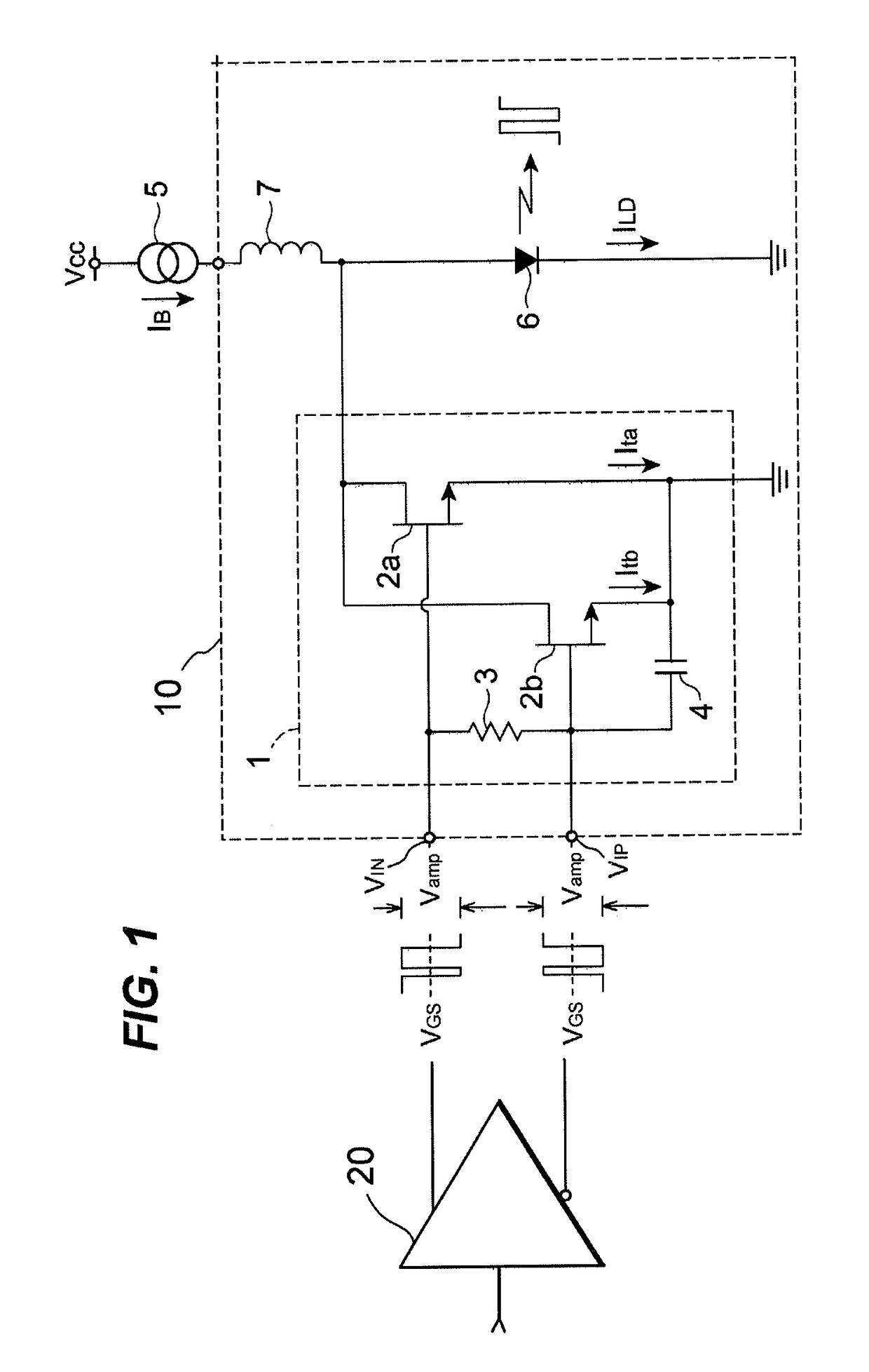
[0016]FIG. 1 shows an exemplary circuit diagram of a laser driver according to an embodiment of the present invention. The laser driver 1 in FIG. 1 includes two FETs 2a and 2b, with the enhancement configuration, a terminator 3, and a capacitor 4, where the laser driver 1 drives a laser diode 6 by shunting a current IB provided from an external current source 5. The laser driver 1 may be driven by a differential circuit 20 connected in the upstream of the laser driver 1. The differential circuit 20, for instance, converts a mono-phase signal provided thereto into signals complementary to each other. One of complementary signals has a normal phase, while, the other of the complementary signals has an opposite phase, thus, the laser driver 1 ma...
PUM
 Abstract
Description
Claims
Application Information