Apparatus for isolated bevel edge clean and method for using the same

a technology of bevel polymer and cleaning apparatus, which is applied in the direction of cleaning equipment, cleaning using tools, chemistry apparatus and processes, etc., can solve the problems of notch, inability to break the strong bond of bevel polymer deposited on the substrate edge, and inability to remove post-etch residues

Inactive Publication Date: 2012-03-06
LAM RES CORP
View PDF41 Cites 8 Cited by
  • Summary
  • Abstract
  • Description
  • Claims
  • Application Information

AI Technical Summary

Benefits of technology

[0008]In one embodiment, an apparatus for cleaning an edge of a substrate is disclosed. The apparatus includes a housing to receive the edge of the substrate. A bristle brush unit with a plurality of outwardly extending vanes is located within the housing. The bristle brush unit is mounted on a rotating shaft within the housing and aligned such that the outwardly extending vanes contact the edge of the substrate when rotating, for efficient cleaning.
[0010]In yet another embodiment, a method is disclosed for cleaning an edge of a substrate. The method includes receiving the edge of the substrate within a housing. A bristle brush unit within the housing is rotated in a direction opposite to an angle of curvature of the outwardly extending vanes. The rotating bristle brush unit assists in cleaning the edge of the substrate.

Problems solved by technology

Semiconductor chip fabrication is a complicated process that involves a coordinated series of fabrication operations.
It is well known that during the various steps of these operations, the surfaces, edges, bevels and notches of the semiconductor substrate (wafer) become contaminated with a layer of residue comprised of particulates, organic materials, metallic impurities, etc.
However, one type of post-etch residue that does not readily lend itself to removal by conventional post-etch chemical-based cleaning methods is organic ‘bevel’ polymer residue found on the substrate bevel edge, notch, and the portion of the backside of the substrate.
These tools are effective at removing some of the contaminants and certain types of residue on the front and back side of the substrate but are not capable of breaking the strong bond of the bevel polymers deposited on the substrate edges and notch.

Method used


Image

  • Apparatus for isolated bevel edge clean and method for using the same
  • Apparatus for isolated bevel edge clean and method for using the same
  • Apparatus for isolated bevel edge clean and method for using the same

Examples


Embodiment Construction

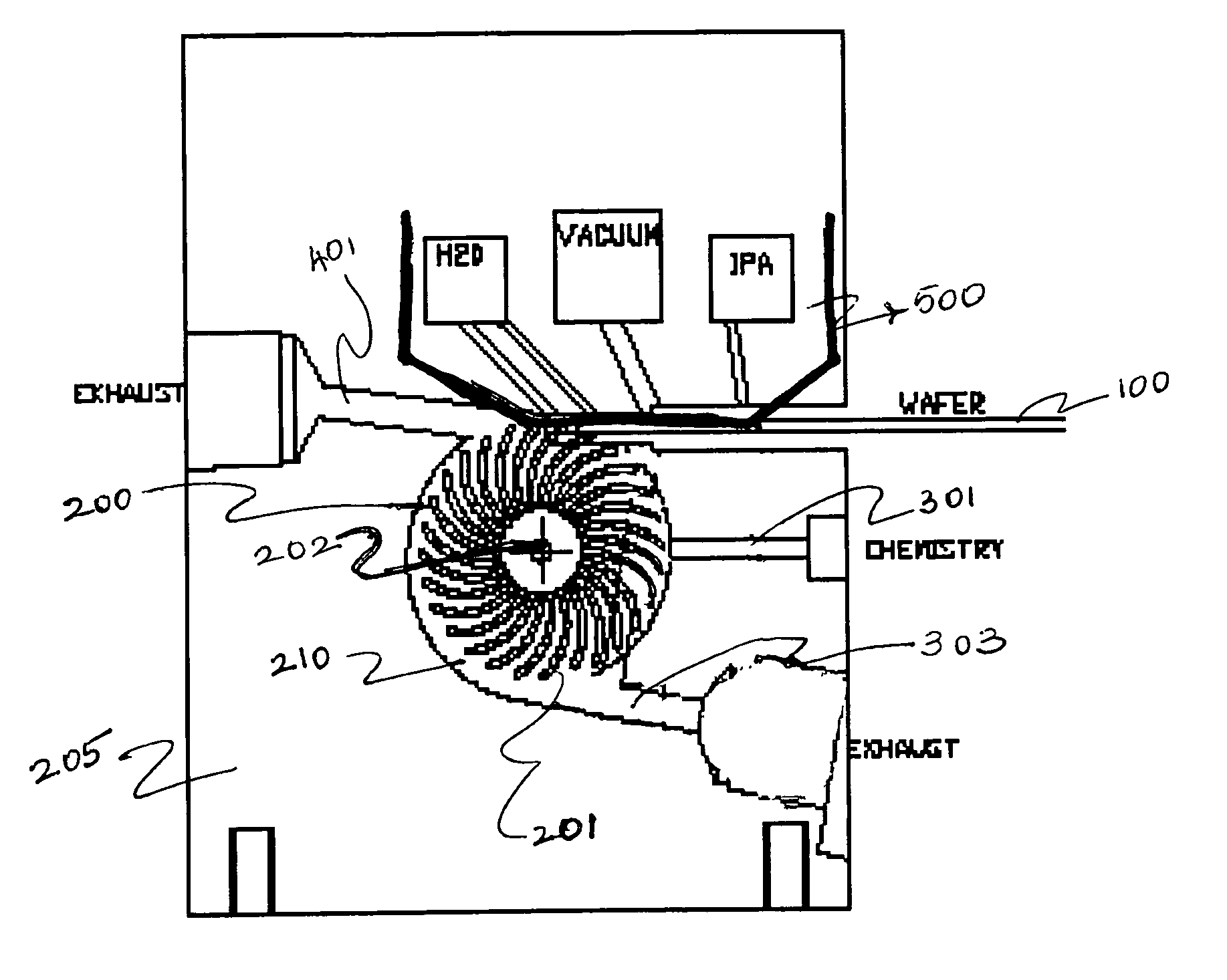
[0020]Several embodiments for an improved and more effective substrate edge cleaning apparatus, system and method will now be described. It will be obvious, however, to one skilled in the art, that the present invention may be practiced without some or all of these specific details. In other instances, well known process operations have not been described in detail in order not to unnecessarily obscure the present invention.

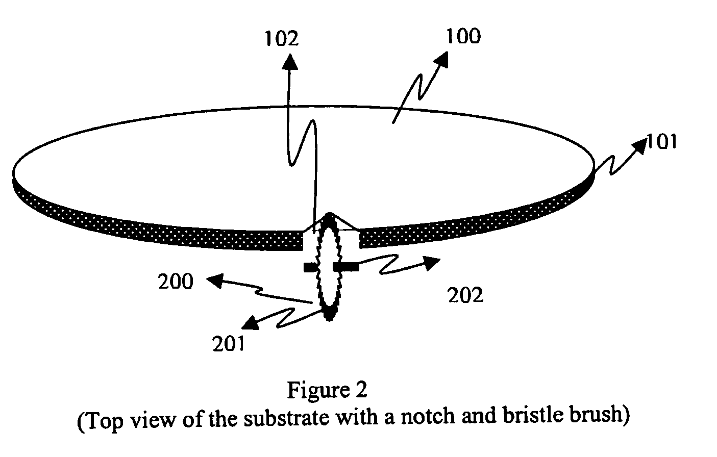
[0021]Substrate edge cleaning apparatus, systems and methods are very important to the ultimate quality of the resulting semiconductor products, e.g., microchips. In the present invention, the bevel polymers deposited on the substrate edges are treated with mechanical and chemical scrubbing that cuts, tears and removes the bevel polymers from the substrate edge.

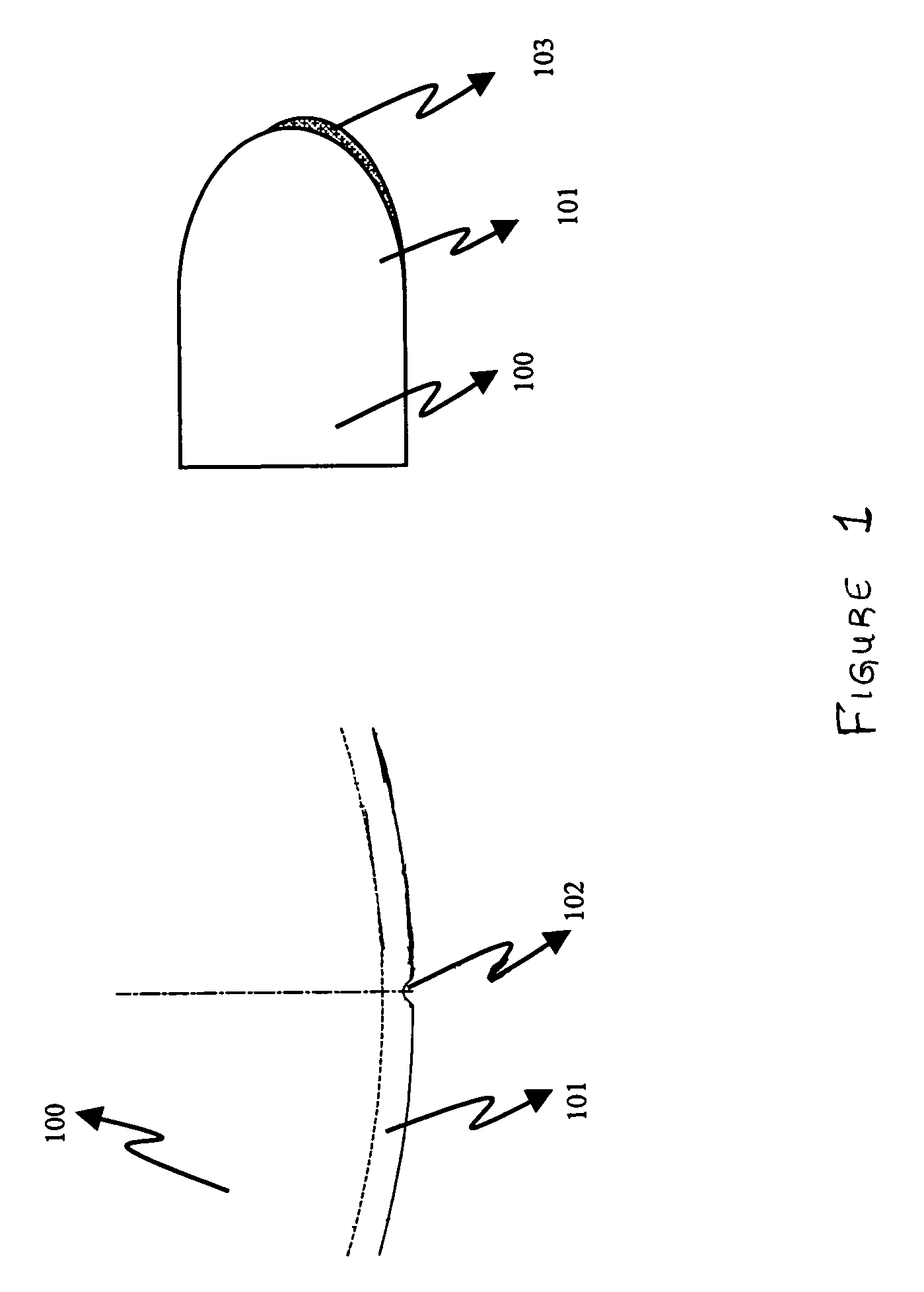
[0022]In this document, a substrate is used to refer to a thin slice of a semi-conductor material (usually silicon), from which microchips are made. The substrate can also be a flat panel substrate, which ...


PUM

PropertyMeasurementUnit
semiconductoraaaaaaaaaa
hardnessaaaaaaaaaa
angleaaaaaaaaaa

Abstract

An apparatus, system and method for cleaning a substrate edge include a bristle brush unit that cleans bevel polymers deposited on substrate edges using frictional contact in the presence of cleaning chemistry. The bristle brush unit is made up of a plurality of outwardly extending vanes and is mounted on a rotating shaft. An abrasive material is distributed throughout and within the outwardly extending vanes of the bristle brush unit to provide the frictional contact. The bristle brush unit cleans the edge of the substrate by allowing frictional contact of the plurality of abrasive particles with the edge of the substrate in the presence of fluids, such as cleaning chemistry, to cut, rip and tear the bevel polymer from the edge of the substrate.

Description

FIELD OF THE INVENTION[0001]The present invention relates generally to semiconductor substrate processing, and more particularly, to a method and apparatus for cleaning substrate edges before, during and after fabrication operations.DESCRIPTION OF THE RELATED ART[0002]Semiconductor chip fabrication is a complicated process that involves a coordinated series of fabrication operations. These operations can be broadly characterized to include steps such as layering, patterning, etching, doping, chemical mechanical polishing (CMP), etc. It is well known that during the various steps of these operations, the surfaces, edges, bevels and notches of the semiconductor substrate (wafer) become contaminated with a layer of residue comprised of particulates, organic materials, metallic impurities, etc. There is a need to clean the surface of the substrate of these contaminated particles in order to maximize the yield of contaminant-free chips.[0003]Some examples of operations that may result in...

Claims


Application Information

Patent Timeline
Patent Type & Authority Patents(United States)
IPC IPC(8): B08B7/00
CPCH01L21/67046Y10S134/902H01L21/304B24B1/00B08B11/02B08B1/04
Inventor YOON, HYUNGSUK ALEXANDERBAILEY, III, ANDREW D.RYDER, JASON A.WILCOXSON, MARK H.GASPARITSCH, JEFFREY G.JOHNSON, RANDYHOFFMANN, STEPHAN P.
Owner LAM RES CORP
Why Eureka
Try Eureka