Nitride semiconductor light emitting device and fabrication method thereof

a light emitting device and semiconductor technology, applied in semiconductor/solid-state device manufacturing, semiconductor devices, semiconductor devices, etc., can solve the problems of increasing the leakage current of the device, gan based light emitting device has a bad static electricity characteristic, and gan thin film is prone to crystal defects. , to achieve the effect of reducing the leakage current, preventing the damage of the light emitting device, and increasing the resistance in the region

a light emitting device and semiconductor technology, applied in semiconductor/solid-state device manufacturing, semiconductor devices, semiconductor devices, etc., can solve the problems of increasing the leakage current of the device, gan based light emitting device has a bad static electricity characteristic, and gan thin film is prone to crystal defects. , to achieve the effect of reducing the leakage current, preventing the damage of the light emitting device, and increasing the resistance in the region

US8129711B2Active Publication Date: 2012-03-06SAMSUNG ELECTRONICS CO LTD

Image

  • Nitride semiconductor light emitting device and fabrication method thereof
  • Nitride semiconductor light emitting device and fabrication method thereof
  • Nitride semiconductor light emitting device and fabrication method thereof

Examples


Embodiment Construction

[0054]Hereinafter, an apparatus for forming a nitride semiconductor light emitting device and a method for forming a fabrication method thereof in accordance with the present invention will be described in detail with reference to the accompanying drawings.

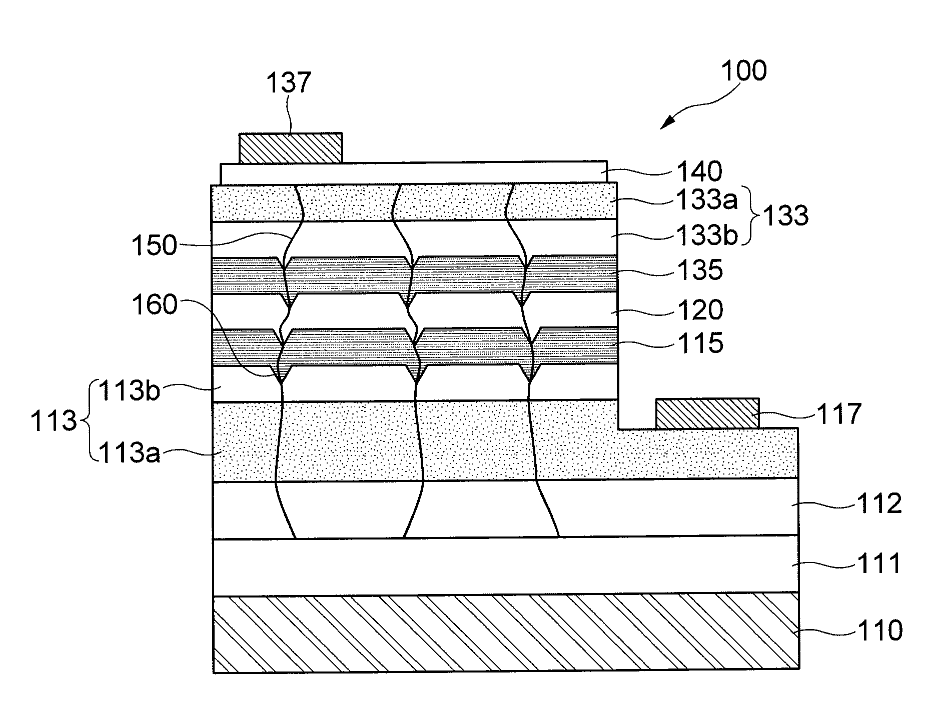
[0055]FIG. 1 is a cross sectional view showing a structure of a nitride semiconductor light emitting device (LED) in accordance with the present invention.

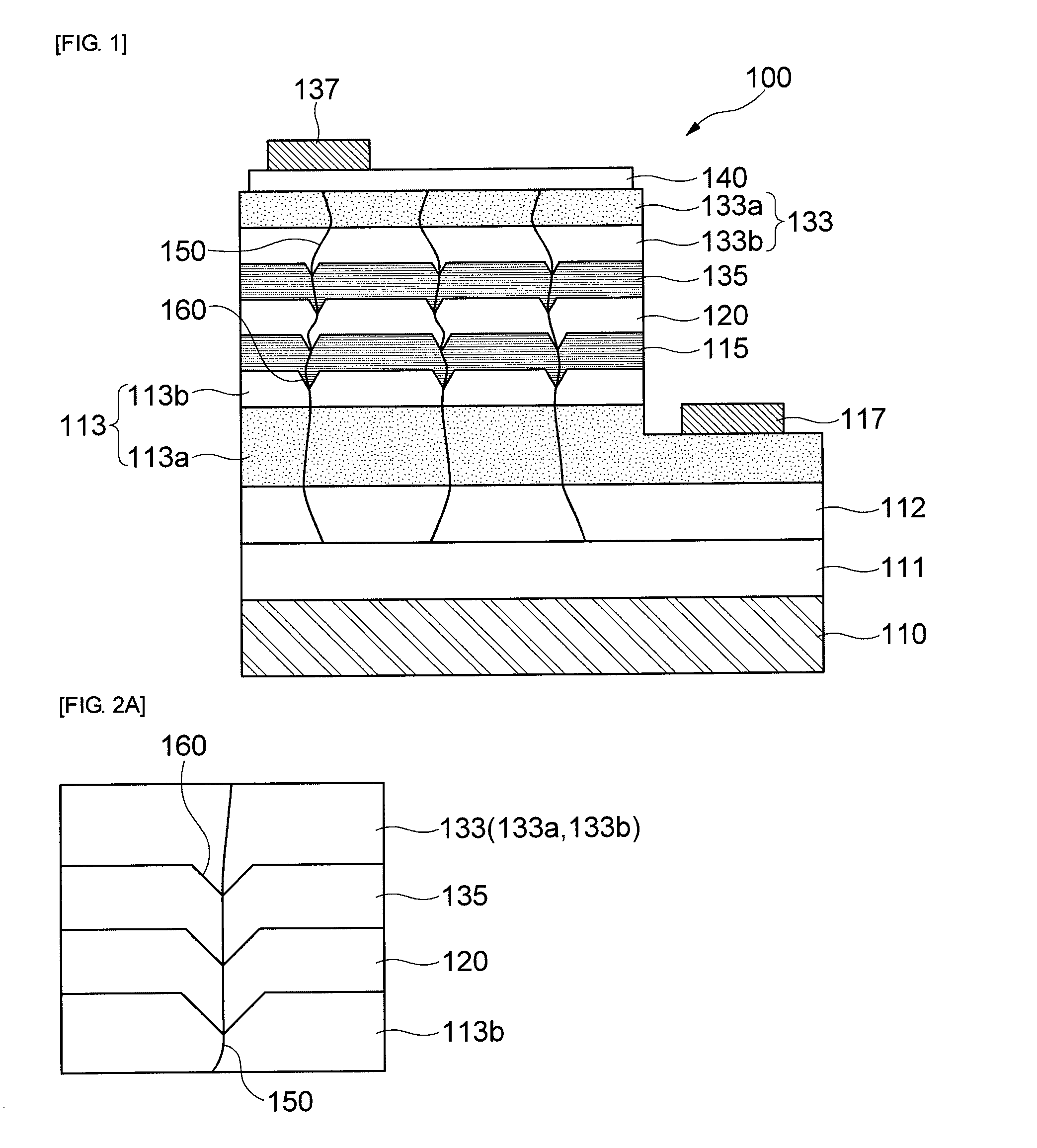
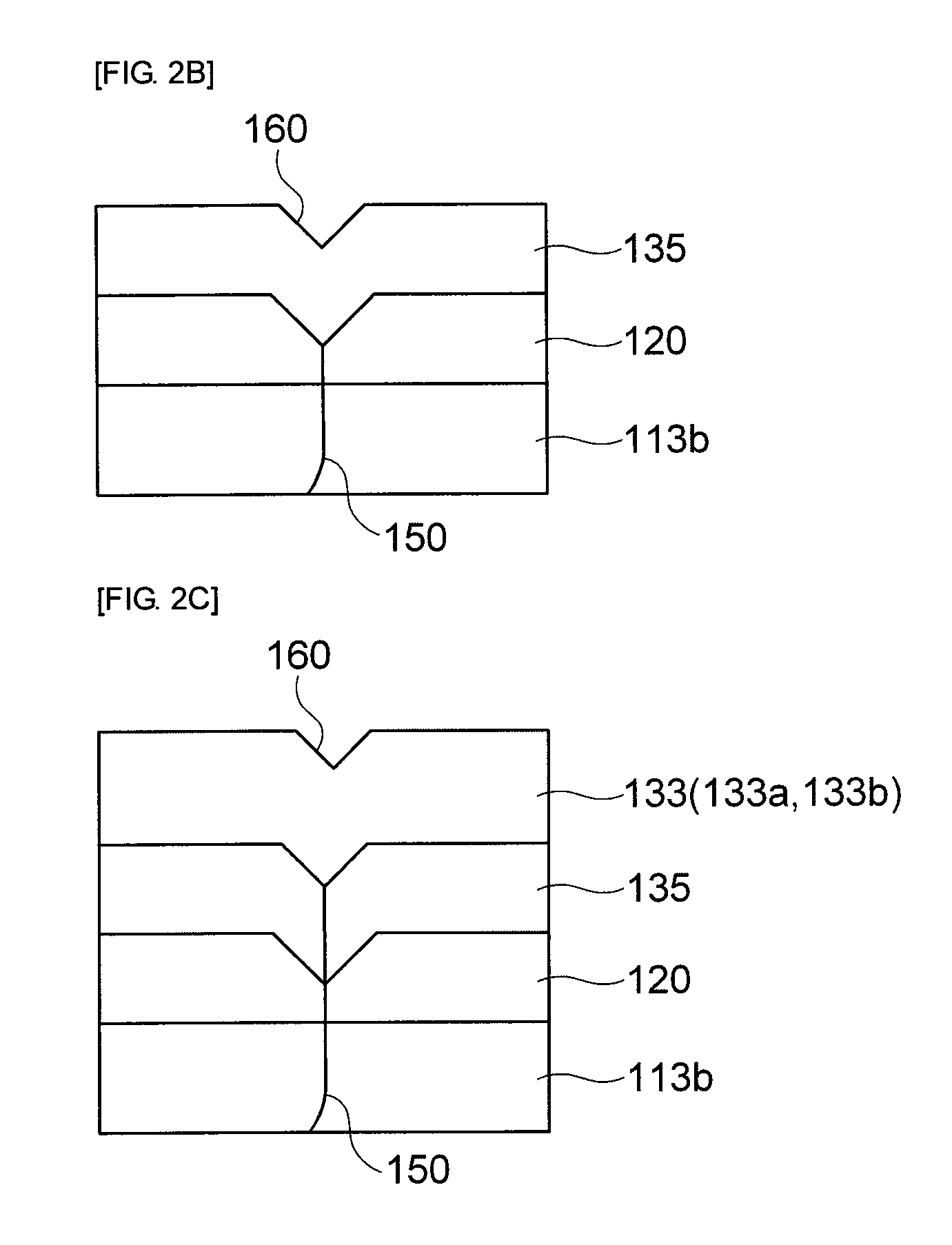
[0056]As shown in FIG. 1, a nitride semiconductor light emitting device 100 in accordance with the present invention includes a substrate 110, a buffer layer 111 formed on the substrate 100, a light emitting structure made of n-type nitride semiconductor layers 113 and 115, an active layer 120 and p-type nitride semiconductor layers 135 and 133 sequentially stacked on the buffer layer 111, and a V-shaped distortion structure layer 160 formed with reference to a penetration defect penetrating into at least one portion of the light emitting structure. At this time, an un-doped GaN...


PUM


Abstract

The present invention relates to a GaN based nitride based light emitting device improved in Electrostatic Discharge (ESD) tolerance (withstanding property) and a method for fabricating the same including a substrate and a V-shaped distortion structure made of an n-type nitride semiconductor layer, an active layer and a p-type nitride semiconductor layer on the substrate and formed with reference to the n-type nitride semiconductor layer.

Description

CROSS-REFERENCE TO RELATED APPLICATIONS[0001]This application claims the benefit of Korean Patent Application No. 10-2007-0070107 filed with the Korea Intellectual Property Office on Jul. 12, 2007, the disclosure of which is incorporated herein by reference.BACKGROUND OF THE INVENTION[0002]1. Field of the Invention[0003]The present invention relates to a nitride semiconductor light emitting device; and, more particularly, to a nitride semiconductor light emitting device capable of improving an ESD (Electrostatic Discharge) tolerance (withstand voltage characteristic) of a GaN based nitride light emitting device and a method for manufacturing the same.[0004]2. Description of the Related Art[0005]Generally, it has been known that a GaN based light emitting device has a bad static electricity characteristic in comparison with other compound light emitting devices. This reason is that a lot of crystal defects are formed in a GaN thin film due to a great lattice mismatch (16%) between a ...

Claims


Application Information

Patent Timeline
06 Mar 2012
Publication
US8129711B2
IPC
H01L29/06; H01L33/22; H01L33/24; H01L33/32
CPC
H01L33/0075; H01L33/24; H01L33/22; H01L33/32
Inventors
KANG, SANG WON; KIM, YONG CHUN