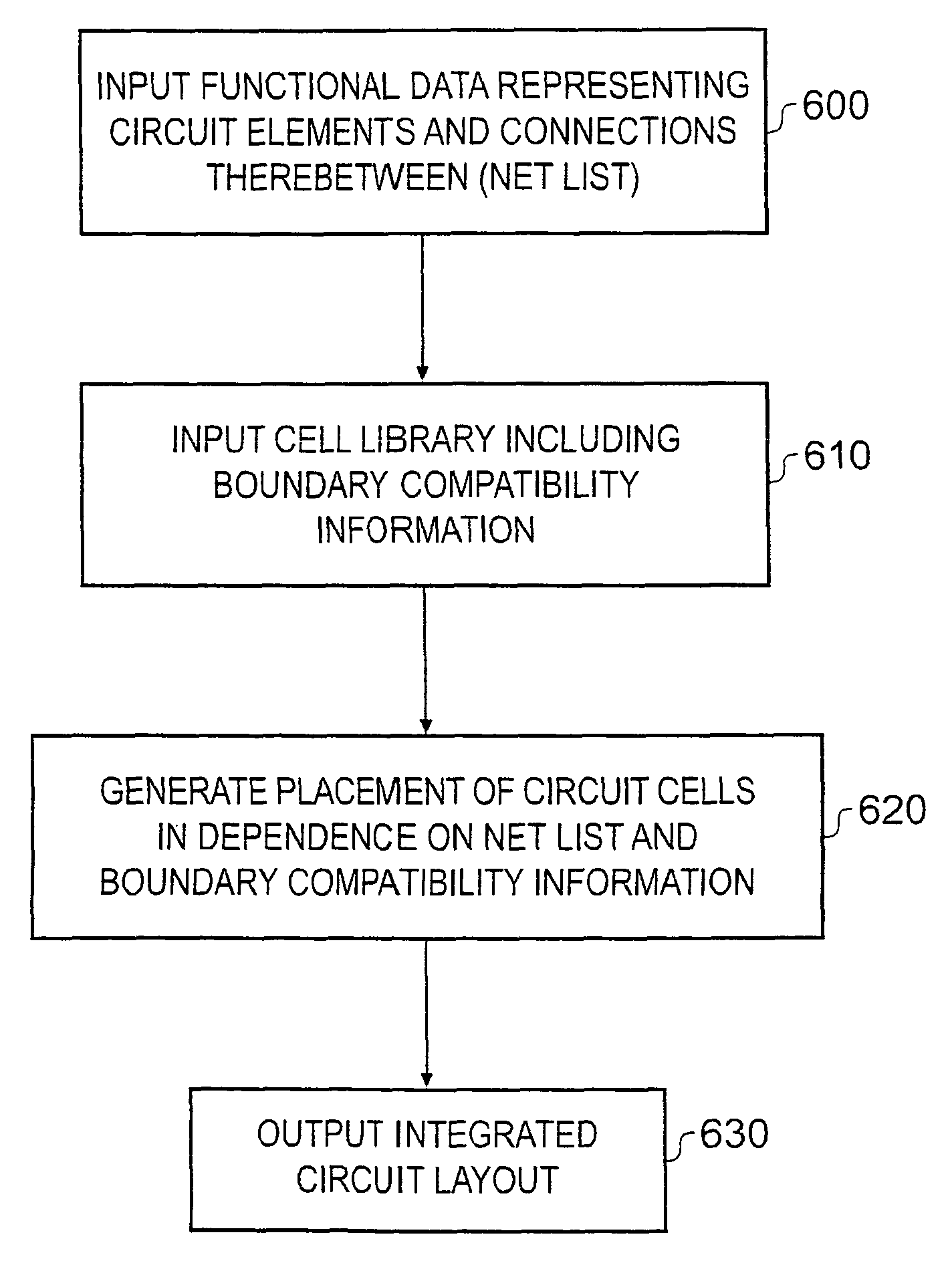
Standard cell placement
a cell placement and standard technology, applied in the field of integrated circuits, can solve problems such as incompatibility between, and achieve the effect of adding decoupling capacitan
- Summary
- Abstract
- Description
- Claims
- Application Information
AI Technical Summary
Benefits of technology
Problems solved by technology
Method used
Image


Examples
Embodiment Construction
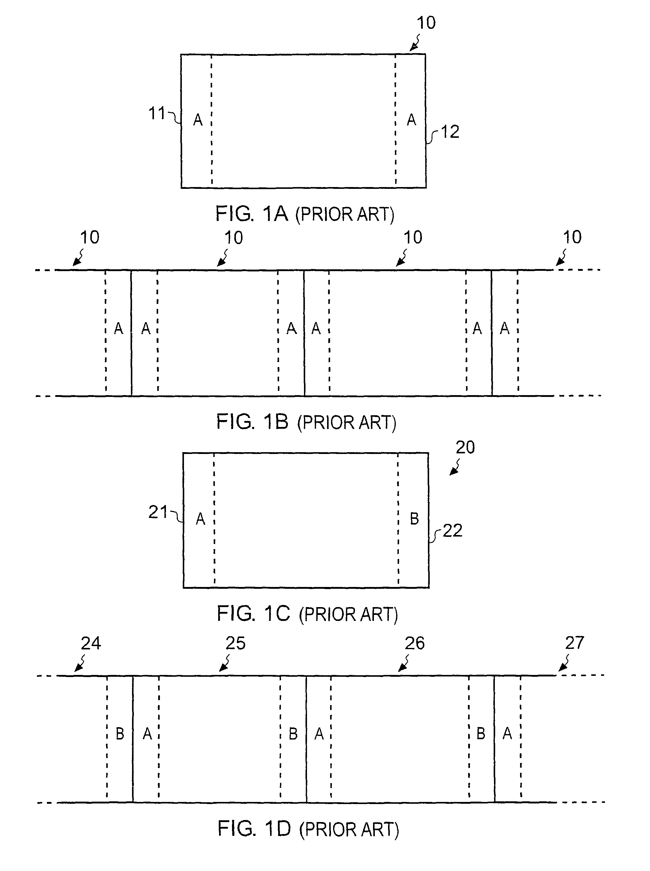
[0039]FIGS. 2A, 2B, 2C and 2D schematically illustrate a set of standard cells according to one example embodiment of the present invention. These standard cells 100, 105, 110, 115 have boundary regions on their left and right delimited by dashed lines 120 and 125 respectively. These boundary regions are as described with reference to FIGS. 1A1B, 1C and 1D, in so far as they represent the limit for elements of the standard cell to approach the left and right boundaries of that standard cell without risking interference with an abutting standard cell. In FIGS. 2A, 2B, 2C and 2D, the example is taken of metal layers 130, 135, 140 and 145 in various arrangements. Thus in this illustrated example the dashed lines 120 and 125 represent the limit for the metal layer to approach the boundaries of the standard cell. In other embodiments the illustrated layers 130, 135, 140 and 145 could be considered to represent other layers of the standard cell such as, for example a polysilicon layer, a ...
PUM
 Abstract
Description
Claims
Application Information