Flash memory device and method of fabricating the same

a flash memory and memory device technology, applied in the direction of semiconductor devices, electrical devices, transistors, etc., can solve the problems of increasing the ratio of faulty devices, reducing the production yield, and reducing the distance between floating gates, so as to improve the interference effect and reduce the distance between cells

Inactive Publication Date: 2012-03-20
SK HYNIX INC
View PDF15 Cites 1 Cited by
  • Summary
  • Abstract
  • Description
  • Claims
  • Application Information

AI Technical Summary

Benefits of technology

[0009]One or more embodiments are directed towards a flash memory device and a method of fabricating the same, which is capable of improving the interference effect and securing the distance between the tunnel oxide layer and the control gate although the distance between cells decreases.

Problems solved by technology

The state of a cell is changed because of the interference effect, which results in an increase in the ratio of faulty devices and a decrease in the production yield.
As the integration degree of semiconductor devices increases, the distance between the floating gates decreases, and the interference becomes an important factor.

Method used


Image

  • Flash memory device and method of fabricating the same
  • Flash memory device and method of fabricating the same
  • Flash memory device and method of fabricating the same

Examples


Embodiment Construction

[0034]Hereinafter, the present disclosure will be described in detail in connection with one or more embodiments with reference to the accompanying drawings.

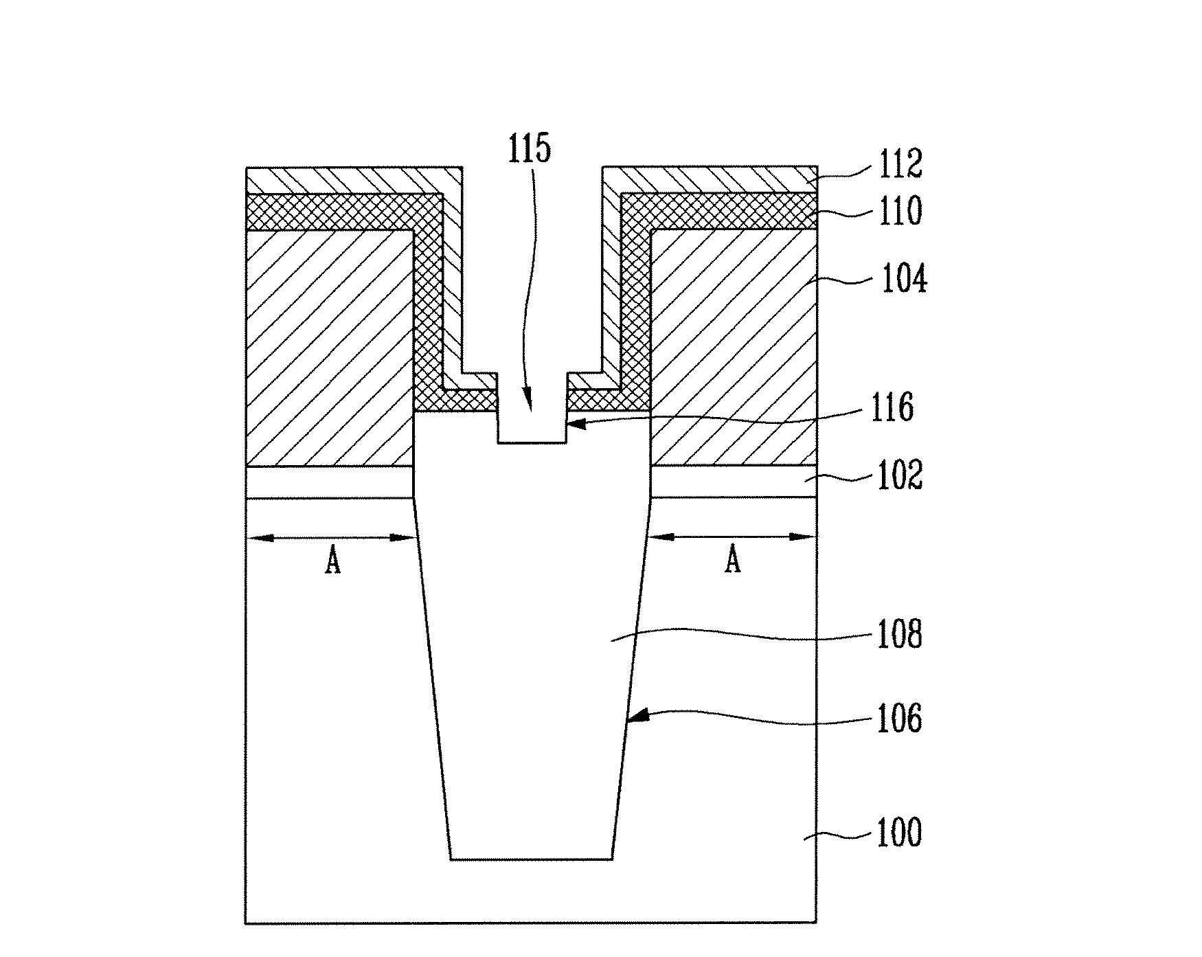
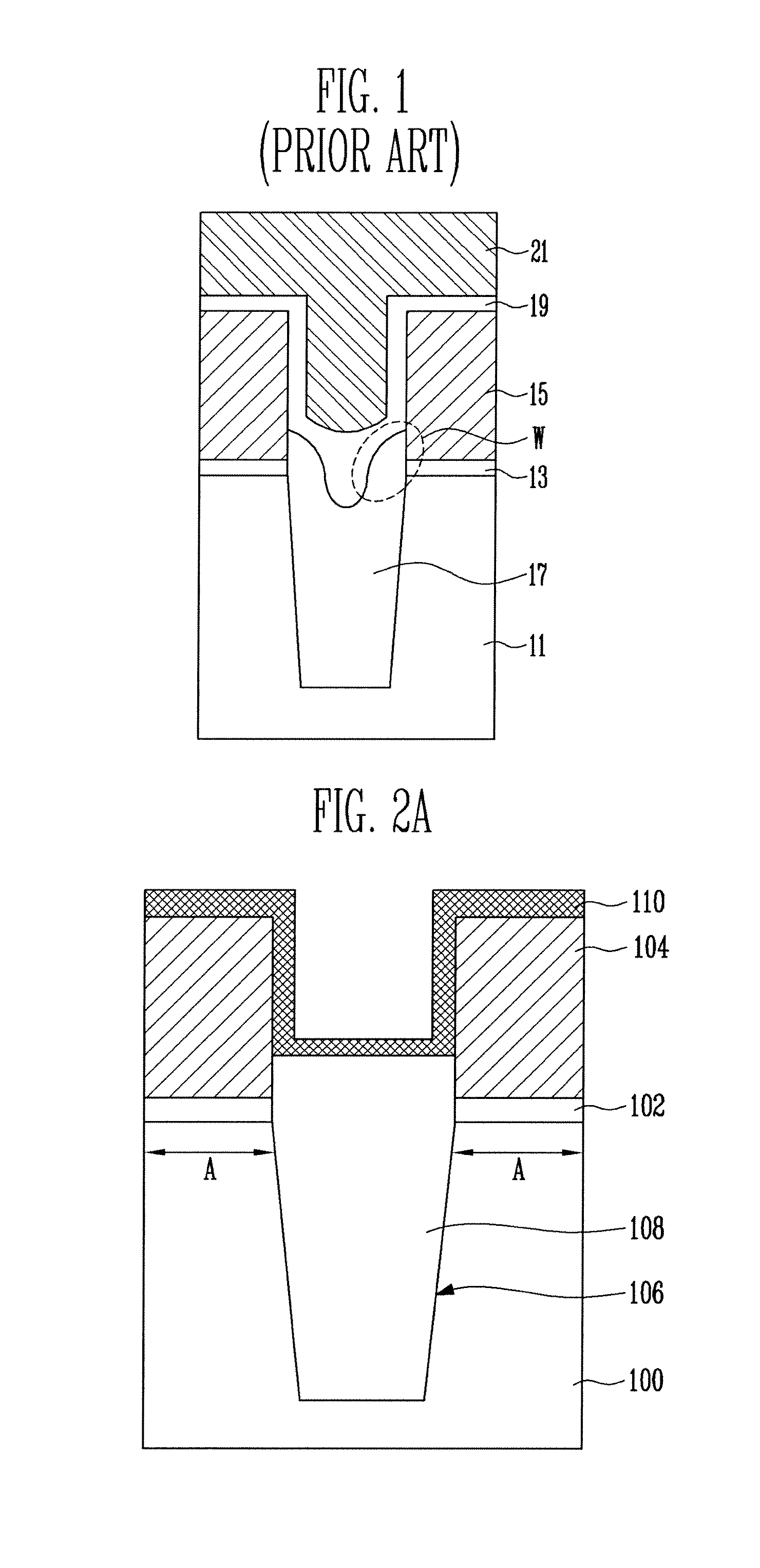
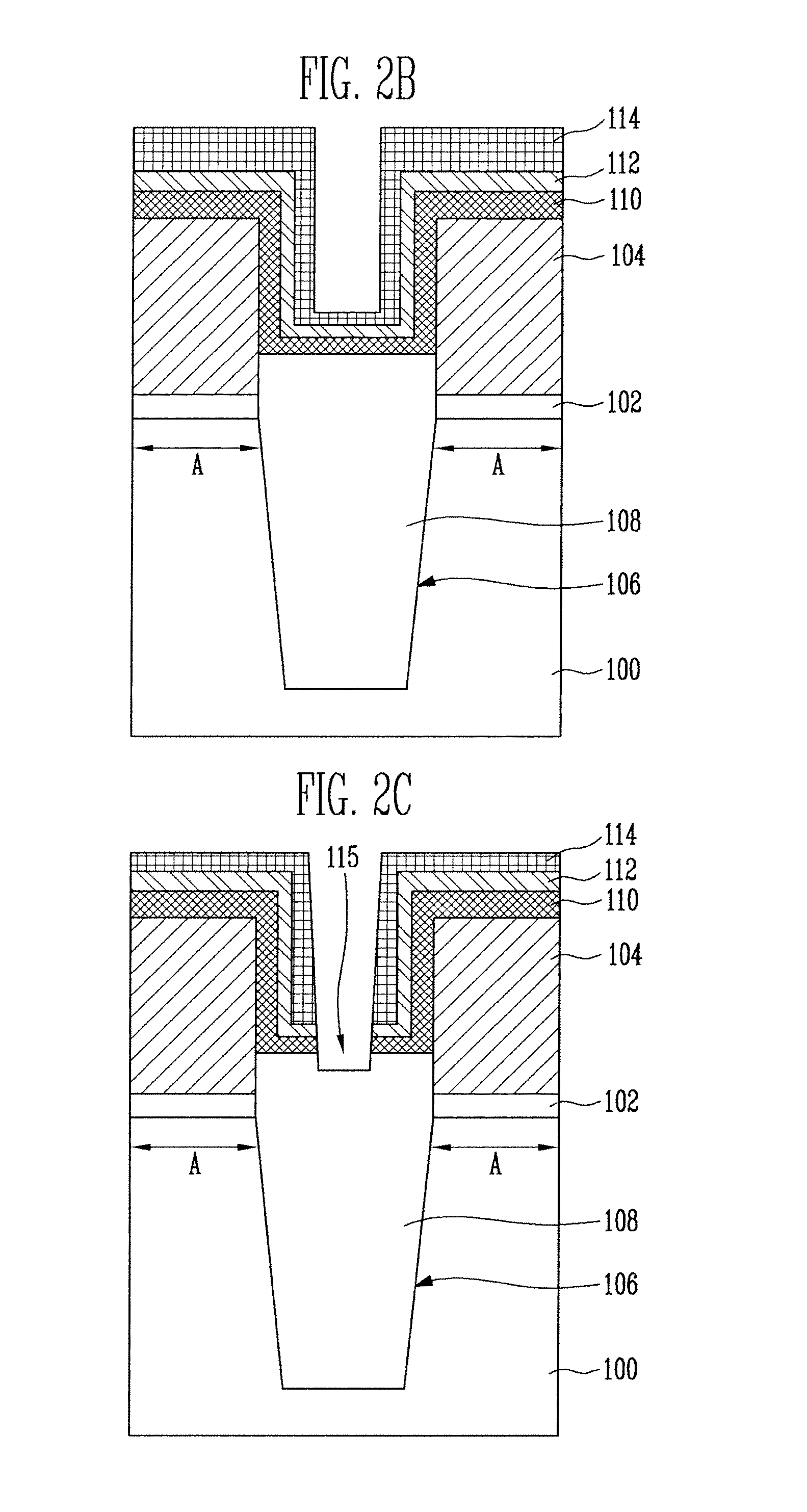
[0035]FIGS. 2A to 2E are sectional views of a flash memory device illustrating a method of fabricating a flash memory device according to one embodiment.

[0036]Referring to FIG. 2A, a semiconductor substrate 100 is provided. Stack layers, each including a tunnel insulating layer 102 and a first conductive layer 104, are formed over respective active regions A of the semiconductor substrate using a known method of fabricating a flash memory device. An isolation layer 108 is formed in the isolation trench 106 of an isolation region of the semiconductor substrate. The sidewalls of the top of the first conductive layer 104 are exposed through the isolation trench 106. The tunnel insulating layer 102 may be formed of a silicon oxide (SiO2) layer. In one exemplary embodiment, the silicon oxide layer may be formed using an oxidation pro...


PUM


Abstract

A flash memory device includes an isolation layer formed on an isolation region of a semiconductor substrate, a tunnel insulating layer formed on an active region of the semiconductor substrate, a first conductive layer formed over the tunnel insulating layer, a dielectric layer formed on the first conductive layer and the isolation layer, a first trench penetrating the dielectric layer on the isolation layer to separate parts of the dielectric layer, a second trench formed on the isolation layer and expanded from the first trench, and a second conductive layer formed over the dielectric layer to fill the first and second trenches.

Description

CROSS-REFERENCES TO RELATED APPLICATIONS[0001]This application claims priority from Korean Patent Application No. 10-2008-0044117, filed on May 13, 2008 and Korean Patent Application No. 10-2009-0006800, filed on Jan. 29, 2009, the contents of which are incorporated herein by reference in their entireties.BACKGROUND[0002]One or more embodiments relate to a flash memory device and a method of fabricating the same, and more particularly, to a flash memory device and a method of fabricating the same, is capable of improving interference effect between neighbor cells and a cycling threshold voltage shift.[0003]In a NAND type flash memory device, a plurality of cells for storing data is electrically connected to each other in series, thereby forming one cell string. A drain selection transistor is formed between the cell string and a drain, and a source selection transistor is formed between the cell string and a source. The cell of the NAND type flash memory device is formed by forming ...

Claims


Application Information

Patent Timeline
Patent Type & Authority Patents(United States)
IPC IPC(8): H01L29/788
CPCH01L21/28273H01L29/42336H01L29/66825H01L29/7881H01L29/40114
Inventor CHO, WHEE WONSO, NAM WOOJEONG, CHEOL MOJANG, LEGAL REPRESENTATIVE, EUN GYEONGKIM, JUNG GEUN
Owner SK HYNIX INC
Why Eureka
Try Eureka