Photo-voltaic cell device and display panel

a photo-voltaic cell and display panel technology, applied in semiconductor devices, solid-state devices, transistors, etc., can solve the problems of easy decay of silicon photo-voltaic cell devices by sunlight or external thermal energy, and achieve the effect of long life and favorable photo-voltaic conversion efficiency

Active Publication Date: 2012-04-10
AU OPTRONICS CORP
View PDF15 Cites 3 Cited by
  • Summary
  • Abstract
  • Description
  • Claims
  • Application Information

AI Technical Summary

Benefits of technology

[0009]In view of the foregoing, the present invention is directed to a photo-voltaic cell device with favorable photo-voltaic conversion efficiency and longer lifetime.
[0010]The present invention is further directed to a display panel capable of integrating the photo-voltaic cell device thereinto and utilizing electric energy obtained during a photo-sensing operation of the photo-voltaic cell device, so as to reduce power consumption.
[0025]To sum up, after the N-type doped silicon-rich dielectric layer is irradiated or after the P-type doped silicon-rich dielectric layer is irradiated, the free electron-hole pairs can be generated. Besides, since the N-type doped silicon-rich dielectric layer and the P-type doped silicon-rich dielectric layer are doped with different ions, an internal electric field exists between the N-type doped silicon-rich dielectric layer and the P-type doped silicon-rich dielectric layer, such that the electrons and the holes are respectively attracted and moved to the P-type doped silicon-rich dielectric layer and the N-type doped silicon-rich dielectric layer. Thus, a spontaneous photo-voltaic current can be generated after the photo-voltaic cell device is irradiated. That is to say, the photo-voltaic cell device of the present invention has favorable photo-voltaic conversion efficiency and longer lifetime with satisfactory structural stability. On the other hand, a required thickness of a film layer in the photo-voltaic cell device is relatively smaller and thinner (e.g. 100 nm˜500 nm), and therefore the photo-voltaic cell device of the present invention is adapted to be integrated into a process of fabricating a display panel. Thereby, the electric energy obtained during a photo-sensing operation of the photo-voltaic cell device can be utilized by the display panel, so as to reduce power consumption.

Problems solved by technology

The silicon photo-voltaic cell device is easily to be decayed by the sunlight or external thermal energy due to silicon recrystalline or rearrangement.

Method used


Image

  • Photo-voltaic cell device and display panel
  • Photo-voltaic cell device and display panel
  • Photo-voltaic cell device and display panel

Examples


first embodiment

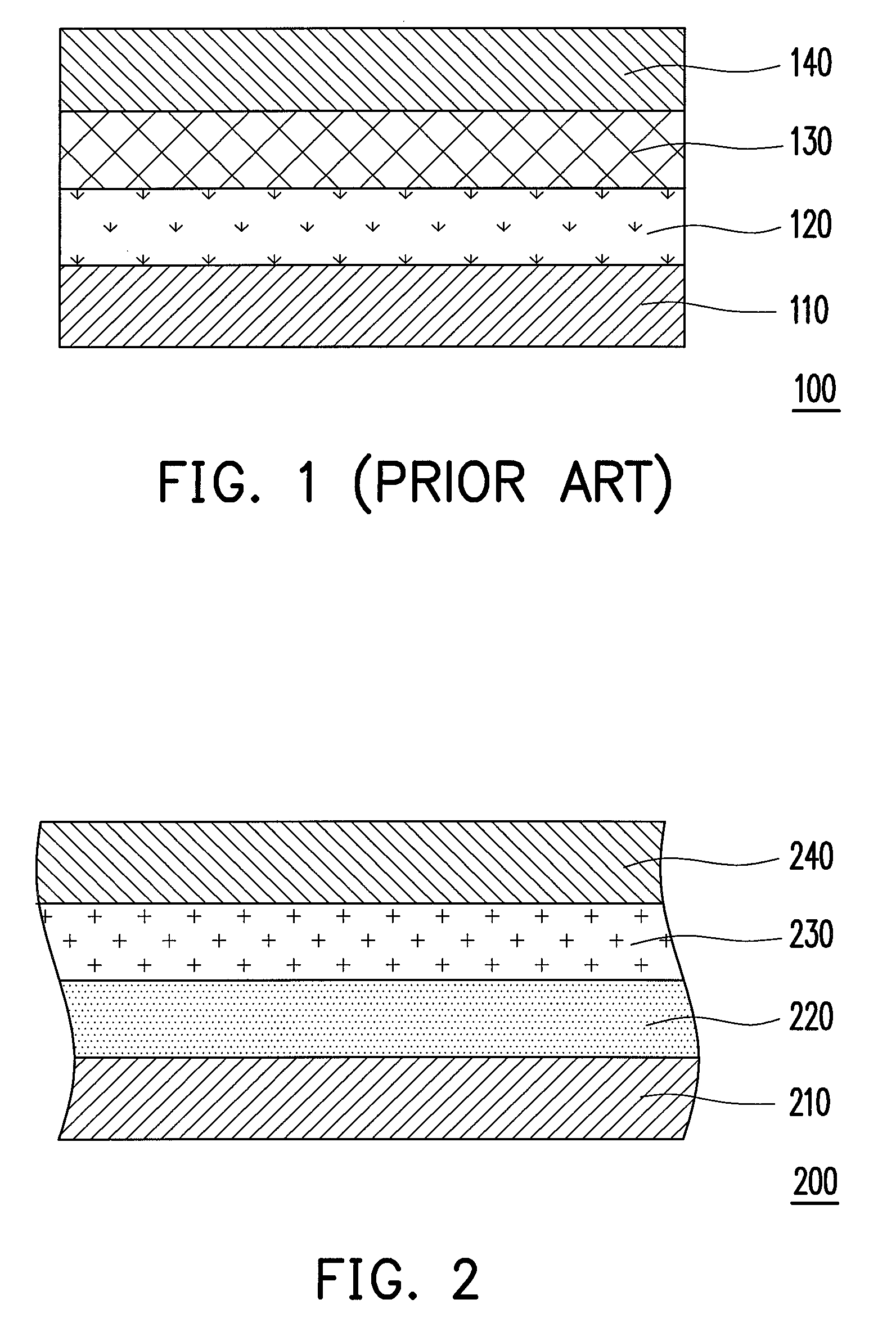
[0035]FIG. 2 is a schematic structural view of a photo-voltaic cell device according to a first embodiment of the present invention. Referring to FIG. 2, the photo-voltaic cell device 200 of the present embodiment includes a first electrode 210, an N-type doped silicon-rich dielectric layer 220, a P-type doped silicon-rich dielectric layer 230, and a second electrode 240. The N-type doped silicon-rich dielectric layer 220 is disposed on the first electrode 210, and the N-type doped silicon-rich dielectric layer 220 is doped with an N-type dopant. The P-type doped silicon-rich dielectric layer 230 is disposed on the N-type doped silicon-rich dielectric layer 220, and the P-type doped silicon-rich dielectric layer 230 is doped with a P-type dopant. The second electrode 240 is disposed on the P-type doped silicon-rich dielectric layer 230.

[0036]Said vertical design can also be changed to a horizontal design or a lateral design (not shown) in an modified embodiment of the present invent...

second embodiment

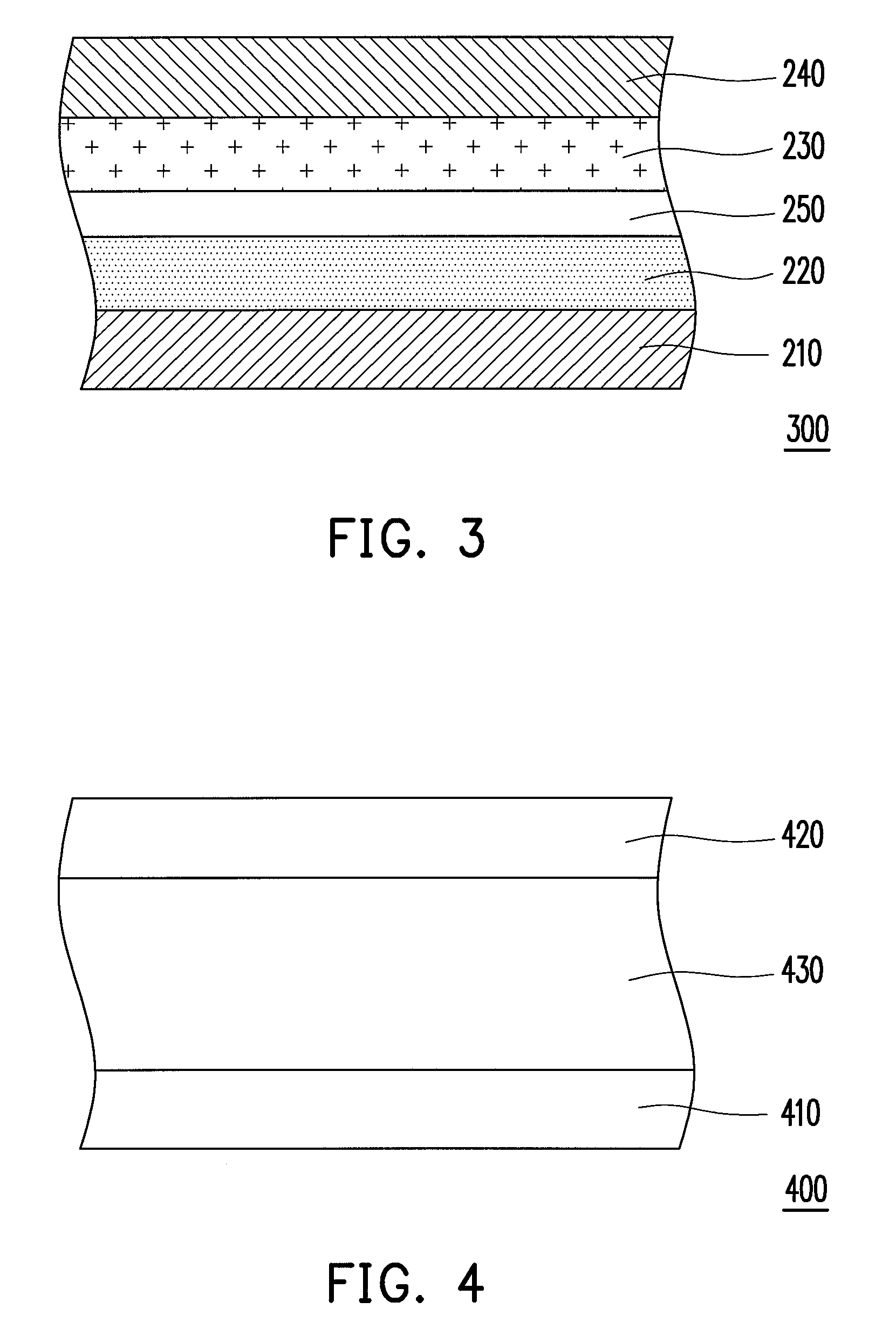
[0049]FIG. 4 is a schematic view of a display panel according to a second embodiment of the present invention. FIG. 5 is a schematic cross-sectional view of a first substrate depicted in FIG. 4. Referring to FIGS. 4 and 5, the display panel 400 of the present embodiment has a pixel region P1 and a sensing region P2. The display panel 400 includes a first substrate 410, a second substrate 420, and a display medium 430 including such as a liquid crystal material, an organic light emitting material, an electrophoretic material, or the like. A pixel array 412 and at least a photo-voltaic cell device 414 are disposed on the first substrate 410. The pixel array 412 is disposed in the pixel region P1 and includes a plurality of TFTs 412a and a plurality of pixel electrodes 412b electrically connected to the TFTs 412a. The photo-voltaic cell device 414 is disposed in the sensing region P2 and includes a first electrode 414a, a first silicon-rich dielectric layer 414b, a second silicon-rich ...

third embodiment

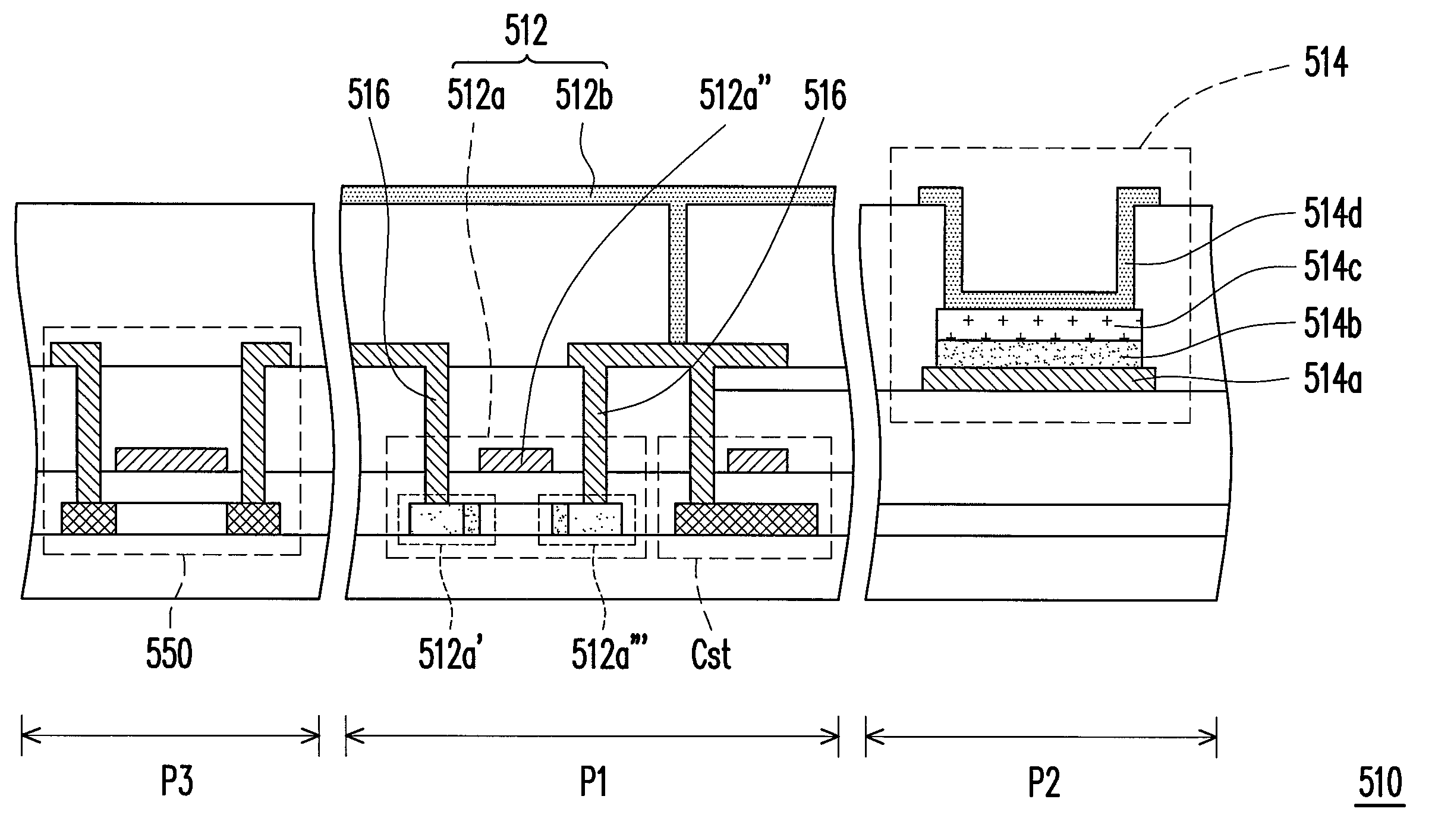
[0059]FIG. 6 is a schematic view of a display panel according to a third embodiment of the present invention. FIG. 7 is a schematic cross-sectional view of a first substrate depicted in FIG. 6. Referring to FIGS. 6 and 7, the display panel 500 of the present embodiment has a pixel region P1 and a sensing region P2. The display panel 500 includes a first substrate 510, a second substrate 520, and a display medium 530. A pixel array 512 and at least a photo-voltaic cell device 514 are disposed on the first substrate 510. The pixel array 512 is disposed in the pixel region P1 and includes a plurality of TFTs 512a and a plurality of pixel electrodes 512b electrically connected to the TFTs 512a. The photo-voltaic cell device 514 is disposed in the sensing region P2 and includes a first electrode 514a, a first silicon-rich dielectric layer 514b, a second silicon-rich dielectric layer 514c, and a second electrode 514d. The first silicon-rich dielectric layer 514b is disposed on the first e...


PUM


Abstract

A photo-voltaic cell device includes a first electrode, an N-type doped silicon-rich dielectric layer, a P-type doped silicon-rich dielectric layer, and a second electrode. The N-type doped silicon-rich dielectric layer is disposed on the first electrode, and the N-type doped silicon-rich dielectric layer is doped with an N-type dopant. The P-type doped silicon-rich dielectric layer is disposed on the N-type doped silicon-rich dielectric layer, and the P-type doped silicon-rich dielectric layer is doped with a P-type dopant. The second electrode is disposed on the P-type doped silicon-rich dielectric layer. A display panel including the photo-voltaic cell device is also provided.

Description

CROSS-REFERENCE TO RELATED APPLICATION[0001]This application claims the priority benefit of Taiwan application serial no. 97150761, filed Dec. 25, 2008. The entirety of the above-mentioned patent application is hereby incorporated by reference herein and made a part of specification.BACKGROUND OF THE INVENTION[0002]1. Field of the Invention[0003]The present invention relates to a photo-voltaic device and a display apparatus, and more particularly to a photo-voltaic cell device and a display panel.[0004]2. Description of Related Art[0005]In general, a photo-voltaic cell device is often made of silicon or group III-V semiconductors. After the photo-voltaic cell device is irradiated, free electron-hole pairs are generated in a material layer of the photo-voltaic cell device, and charges are separated because of electric field effects, so as to form a semiconductor device having a voltage difference caused by the electric field effects. Operation principles of the photo-voltaic cell dev...

Claims


Application Information

Patent Timeline
Patent Type & Authority Patents(United States)
IPC IPC(8): H01L29/786
CPCH01L31/032H01L31/075H01L31/0384Y02E10/548Y02E10/547
Inventor CHO, AN-THUNGPENG, CHIA-TIENCHEN, YU-CHENGLIN, HONG-ZHANGWEN, YI-CHIENSUN, WEI-MINHUNG, CHI-MAOCHEN, CHUN-HSIUN
Owner AU OPTRONICS CORP
Why Eureka
Try Eureka