Solid-state imaging device and driving method thereof
a solid-state imaging and driving method technology, applied in the direction of semiconductor devices, radio frequency controlled devices, electrical devices, etc., can solve the problems of degrading charge transfer efficiency, achieve the effect of improving charge transfer efficiency, suppressing the generation of dark current, and improving charge transfer efficiency
- Summary
- Abstract
- Description
- Claims
- Application Information
AI Technical Summary
Benefits of technology
Problems solved by technology
Method used
Image
Examples
first embodiment
[First Embodiment]
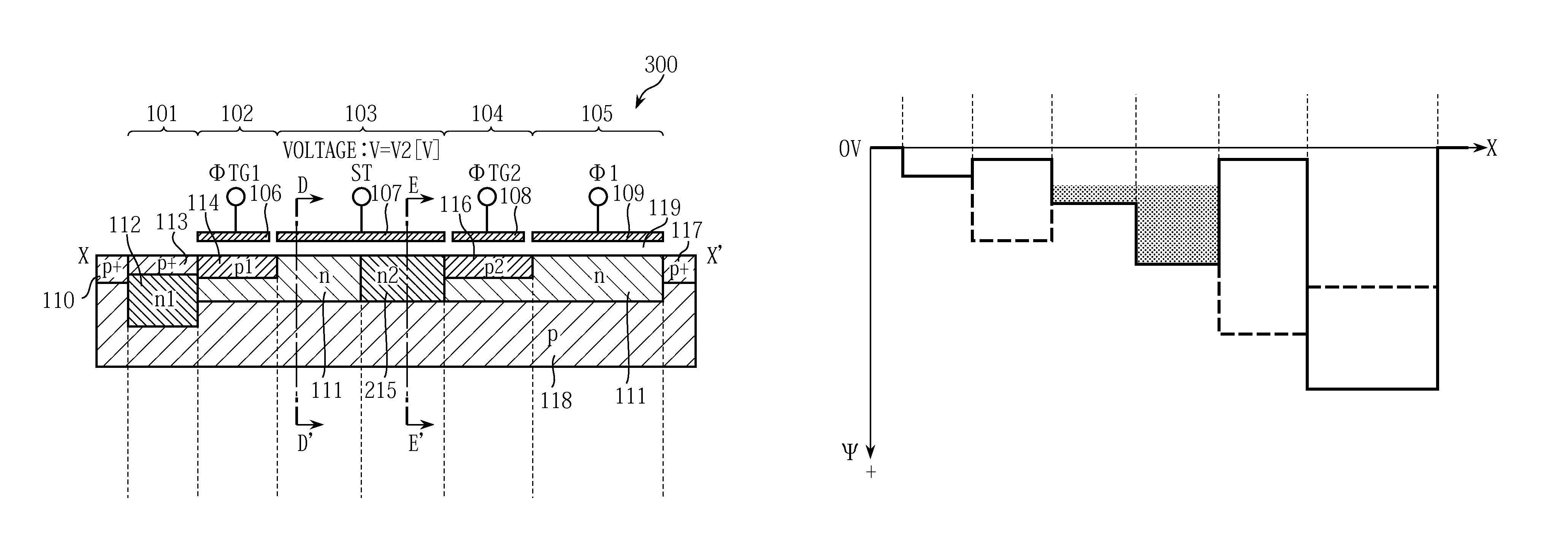
[0074]The solid-state imaging device 40 has a photoelectric conversion section (or photodiode) 1 including an n-type diffusion layer 12 with the impurity concentration of n1, a charge transfer gate section 2 including a charge transfer gate electrode 6, a charge storage section 3 including a charge storage gate electrode 7, a charge transfer gate section 4 including a charge transfer gate electrode 8, and a CCD section 5 including a CCD region 21. In the solid-state imaging device 40, the charge transfer gate section 2 is interposed between the photoelectric conversion section (e.g. photodiode) 1 and the charge storage section 3. The charge transfer gate section 4 is interposed between the charge storage section 3 and the CCD section 5. The CCD section 5 is provided with a set of a CCD section gate electrode 9, a CCD section gate electrode 20, a CCD section gate electrode 25, and a CCD section gate electrode 26 for a change transfer row, and an output amplifier 22 ...
second embodiment
[Second Embodiment]
[0112]A second embodiment of the present invention will be described below. FIG. 15A shows a cross section of the solid-state imaging device 40 according to the second embodiment. FIG. 15B shows a transition state of potential wells in the cross section. A solid line and a broken line in FIG. 15B show a potential transition state in response to a voltage applied to each of the electrodes. It should be noted that a plan view of the solid-state imaging device 40 according to the second embodiment is the same as that of the first embodiment. As shown in FIG. 15A, the solid-state imaging device 40 according to the second embodiment has three regions under the charge storage gate electrode 7: the n-type diffusion layer 11 with the impurity concentration of n, the n-type diffusion layer 15 with the impurity concentration of n2 and an n-type diffusion layer 15a with the impurity concentration of n3. The n-type diffusion layer 11 is the region with the impurity concentrat...
third embodiment
[Third Embodiment]
[0123]A third embodiment of the present invention will be described below. FIG. 17A shows a cross section of the solid-state imaging device 40 according to the third embodiment. FIG. 17B shows a transition state of potential wells in the cross section. A solid line and a broken line in FIG. 17B show a potential transition state in response to a voltage applied to each of the electrodes. It should be noted that a plan view of the solid-state imaging device 40 according to the third embodiment is the same as that of the first embodiment or the second embodiment. As shown in FIG. 17A, in the solid-state imaging device 40 according to the third embodiment, two regions of an n-type diffusion layer 15b with the impurity concentration of n4 and an n-type diffusion layer 15c with the impurity concentration of n5 are formed under the charge storage gate electrode 7. It is assumed that the following condition is satisfied between the impurity concentration of n4 and the impu...
PUM
 Abstract
Description
Claims
Application Information


